Processing and manufacturing method of PCB (Printed Circuit Board) and PCB
A PCB board and manufacturing method technology, applied in the direction of electrical components, multi-layer circuit manufacturing, printed circuit manufacturing, etc., can solve the problems that the machine cannot be transferred, the laser aperture is limited, and blind cutting cannot be manufactured, etc., to break through the limitations of laser technology , Fast production and processing, saving production and processing time
- Summary
- Abstract
- Description
- Claims
- Application Information
AI Technical Summary
Problems solved by technology
Method used
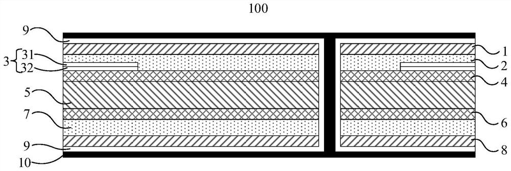
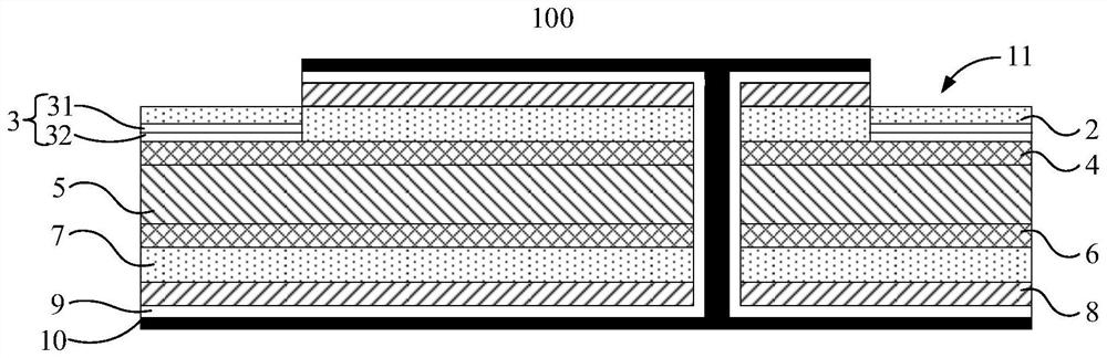
Image


Examples
Embodiment Construction
[0022] The present invention will be further described in detail below with reference to the accompanying drawings and embodiments. It is particularly pointed out that the following examples are only used to illustrate the present invention, but do not limit the scope of the present invention. Likewise, the following embodiments are only some rather than all embodiments of the present invention, and all other embodiments obtained by those of ordinary skill in the art without creative work fall within the protection scope of the present invention.
[0023] Reference herein to an "embodiment" means that a particular feature, structure, or characteristic described in connection with the embodiment can be included in at least one embodiment of the present invention. The appearances of the phrase in various places in the specification are not necessarily all referring to the same embodiment, nor a separate or alternative embodiment that is mutually exclusive of other embodiments. ...
PUM
 Abstract
Description
Claims
Application Information
 - Generate Ideas
- Intellectual Property
- Life Sciences
- Materials
- Tech Scout
- Unparalleled Data Quality
- Higher Quality Content
- 60% Fewer Hallucinations
Browse by: Latest US Patents, China's latest patents, Technical Efficacy Thesaurus, Application Domain, Technology Topic, Popular Technical Reports.
© 2025 PatSnap. All rights reserved.Legal|Privacy policy|Modern Slavery Act Transparency Statement|Sitemap|About US| Contact US: help@patsnap.com