Silicon rod cutting method, device and system

A technology for cutting equipment and cutting methods, applied in stone processing equipment, manufacturing tools, fine working devices, etc., can solve the problems of cross-sectional damage, defects, and high requirements of small silicon wafers, so as to improve cutting efficiency and reduce waste of raw materials , Improve the effect of product quality

Pending Publication Date: 2022-05-10
QINGDAO GAOCE TECH CO LTD
View PDF0 Cites 0 Cited by
  • Summary
  • Abstract
  • Description
  • Claims
  • Application Information

AI Technical Summary

Problems solved by technology

[0003] In the traditional solution, the small monocrystalline silicon cells are usually first cut into large silicon wafers from single crystal silicon rods, and then use laser technology to scribe and cut the large silicon wafers to form small silicon wafers, but in the process of laser scribing , will cause damage and defect states to the cross-section of the small silicon wafer, seriously affecting the conversion efficiency of the final processed heterojunction cell
[0004] The size of silicon rods is getting bigger and bigger, from 166mm to 182mm, and then to 210mm, and may reach 230mm or even 250mm in the future. high, easily broken

Method used


Image

  • Silicon rod cutting method, device and system
  • Silicon rod cutting method, device and system
  • Silicon rod cutting method, device and system

Examples


Embodiment Construction

[0061] In order to make the technical solutions and advantages in the embodiments of the present application clearer, the exemplary embodiments of the present application will be further described in detail below in conjunction with the accompanying drawings. Apparently, the described embodiments are only part of the embodiments of the present application, and Not an exhaustive list of all embodiments. It should be noted that, in the case of no conflict, the embodiments in the present application and the features in the embodiments can be combined with each other.

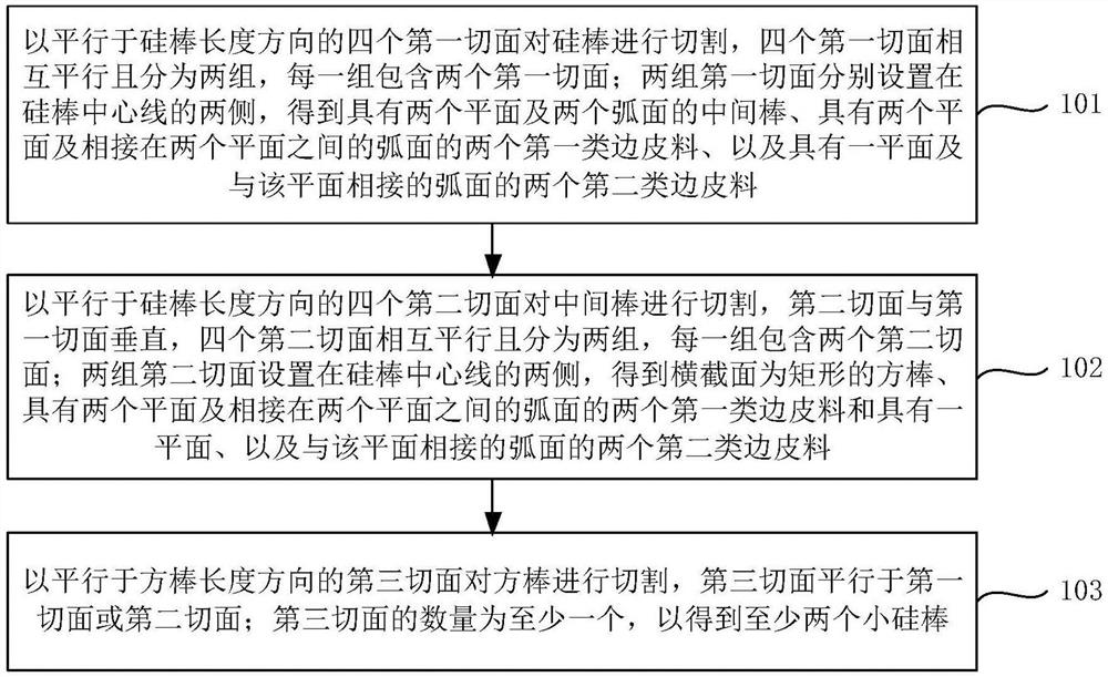
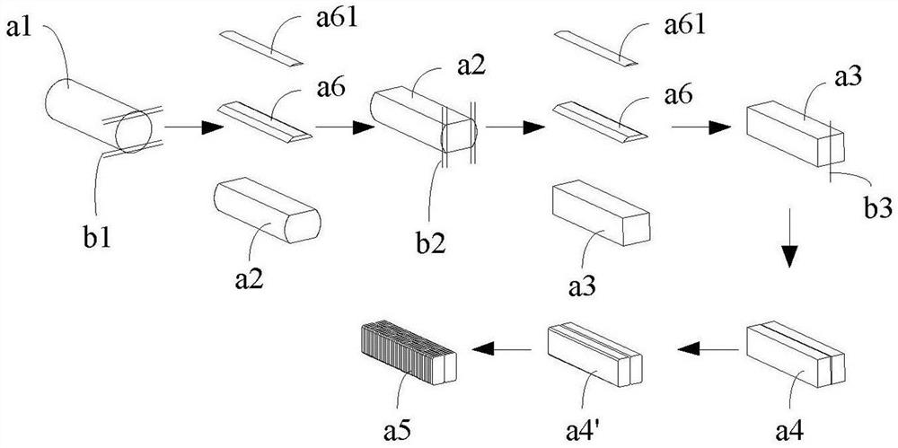
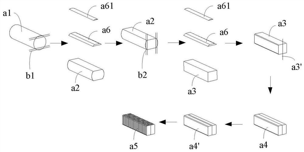
[0062] This embodiment provides a method for cutting silicon rods, which is used for cutting silicon rods to obtain small silicon chips. The silicon rod can be made of polycrystalline silicon material, single crystal silicon material, etc. In this embodiment, only single crystal silicon material is taken as an example to describe the cutting method in detail. Those skilled in the art can directly apply the technic...


PUM

PropertyMeasurementUnit
thicknessaaaaaaaaaa

Abstract

The embodiment of the invention provides a silicon rod cutting method, device and system, and the method comprises the steps: cutting a silicon rod through four first cutting surfaces parallel to the length direction of the silicon rod, and obtaining a middle rod with two planes and two cambered surfaces, two first-class edge leather materials and two second-class edge leather materials; four second tangent planes parallel to the length direction of the silicon rod are used for cutting the middle rod, the second tangent planes are perpendicular to the first tangent planes, and a square rod with the rectangular cross section, two first-class edge leather materials and two second-class edge leather materials are obtained; and the square rod is cut by a third section parallel to the length direction of the square rod, the third section is parallel to the first section or the second section, and at least two small silicon rods are obtained. The embodiment of the invention provides a silicon rod cutting method, equipment and system. The defects caused by cutting a large-piece structure into a small-piece structure in a traditional scheme can be overcome.

Description

technical field [0001] The present application relates to hard and brittle material cutting technology, in particular to a silicon rod cutting method, equipment and system. Background technique [0002] With the development of heterojunction solar cells, the market demand for small silicon wafers is increasing, and the demand for thin wafers is also increasing. The thickness ranges from 180 microns to 150 microns. The future market may require 90 microns, or even 70 microns. , 80 micron thickness silicon wafer, and the thinner the silicon wafer, the smaller the silicon wafer specification is required to ensure the cutting quality and process. [0003] In the traditional solution, the small monocrystalline silicon cells are usually first cut into large silicon wafers from single crystal silicon rods, and then use laser technology to scribe and cut the large silicon wafers to form small silicon wafers, but in the process of laser scribing , will cause damage and defect states...

Claims


Application Information

Patent Timeline
Patent Type & Authority Applications(China)
IPC IPC(8): B28D5/04B28D5/00B24B1/00
CPCB28D5/045B28D5/00B24B1/00
Inventor 薛俊兵李林周波陈明一
Owner QINGDAO GAOCE TECH CO LTD
Why Eureka
Try Eureka