Wafer loading and unloading system and loading and unloading method

A wafer and unloading technology, applied in the direction of conveyor objects, transportation and packaging, etc., can solve the problems of long loading and unloading time of wafers, affecting wafer production efficiency, increasing equipment manufacturing costs, etc., to reduce manufacturing costs and post-processing Effects of maintenance cost, reduction of wafer loading and unloading time, and improvement of production efficiency

Pending Publication Date: 2022-04-01
XIAN ESWIN MATERIAL TECH CO LTD +1
View PDF8 Cites 3 Cited by
  • Summary
  • Abstract
  • Description
  • Claims
  • Application Information

AI Technical Summary

Problems solved by technology

[0002] At present, in the automatic loading and unloading system of wafer double-sided polishing equipment, the unloading buffer area is fixed, and a separate mechanical arm needs to be added to transfer the polished wafers in the unloading buffer area to the wafer cassette. The increase will correspondingly increase the equipment manufacturing cost, and the later maintenance cost will also increase
[0003] On the other hand, in the existing automatic loading and unloading system of wafer double-sided polishing equipment, both the loading robot and the unloading robot can only complete the loading and unloading process by single-chip transfer, so the loading and unloading time of the wafer is relatively long , which seriously affects the production efficiency of the wafer

Method used


Image

  • Wafer loading and unloading system and loading and unloading method
  • Wafer loading and unloading system and loading and unloading method
  • Wafer loading and unloading system and loading and unloading method

Examples


Embodiment Construction

[0020] The following will clearly and completely describe the technical solutions in the embodiments of the present invention with reference to the drawings in the embodiments of the present invention.

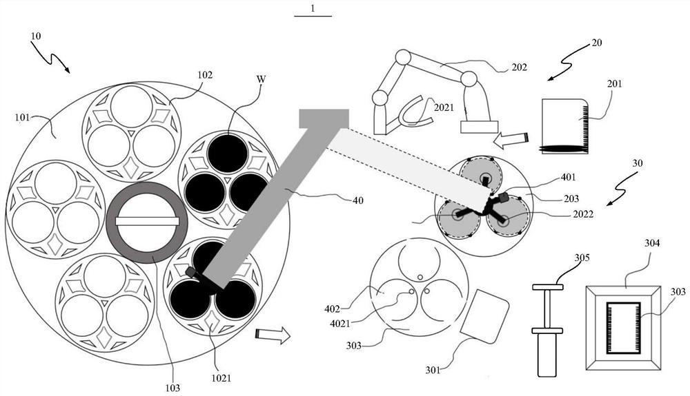
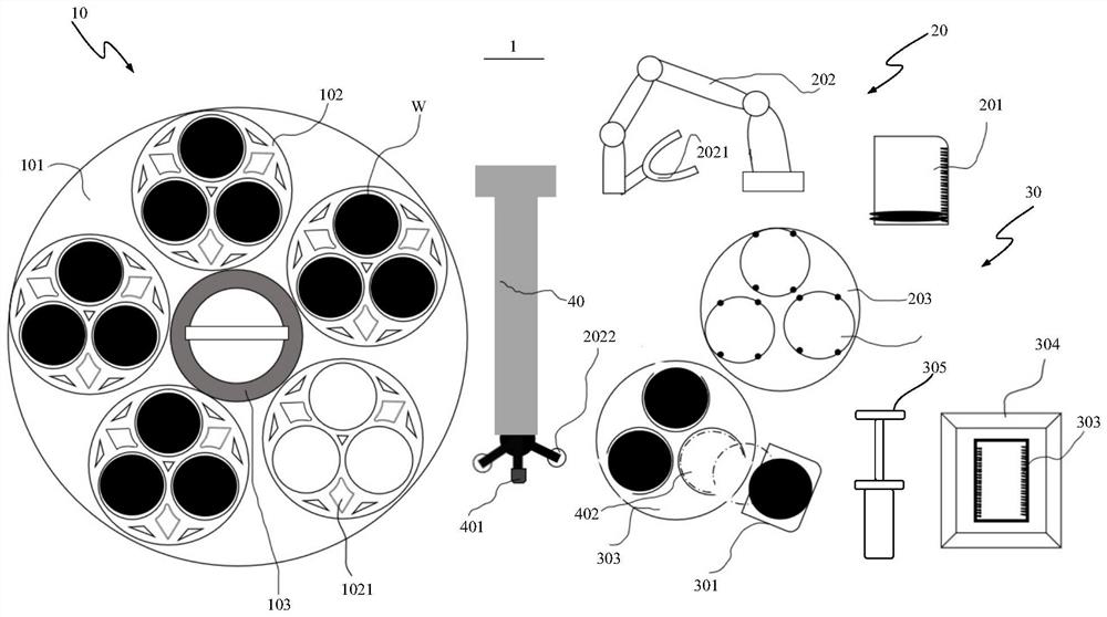
[0021] see figure 1 , which shows the wafer loading and unloading system 1A used when the wafer W is polished on both sides in the conventional technical solution, as figure 1 As shown, the wafer loading and unloading system 1A specifically includes: a carrier device 10, a loading area 20A and an unloading area 30A; wherein,

[0022] Carrier 10 includes grinding disc 101, a plurality of carriers 102 and inner pin ring 103 arranged on grinding disc 101; Used to fix the wafer W, the inner pin ring 103 is used to drive the carrier 102 to rotate, thereby polishing the wafer W through the rotation of the grinding disc 101 and the carrier 102; wherein, each carrier 102 is provided with a carrier identification hole 1021;

[0023] The loading area 20A includes a first wafer casset...


PUM


Abstract

The embodiment of the invention discloses a wafer feeding and discharging system and a wafer feeding and discharging method. The wafer feeding and discharging system comprises a feeding buffer area, a polishing buffer area and a feeding buffer area, wherein the feeding buffer area can temporarily store a plurality of wafers to be polished; the blanking buffer area can temporarily store a plurality of polished wafers; the swinging mechanical arm is used for simultaneously transferring the plurality of wafers to be polished, which are temporarily stored in the feeding buffer area, into the corresponding carriers; and the multiple polished wafers in each carrier are transferred to the discharging cache region at the same time.

Description

technical field [0001] The embodiments of the present invention relate to the technical field of semiconductors, and in particular to a wafer loading and unloading system and a loading and unloading method. Background technique [0002] At present, in the automatic loading and unloading system of wafer double-sided polishing equipment, the unloading buffer area is fixed, and a separate mechanical arm needs to be added to transfer the polished wafers in the unloading buffer area to the wafer cassette. The increase will correspondingly increase the equipment manufacturing cost, and the subsequent maintenance cost will also increase. [0003] On the other hand, in the existing automatic loading and unloading system of wafer double-sided polishing equipment, both the loading robot and the unloading robot can only complete the loading and unloading process by single-chip transfer, so the loading and unloading time of the wafer is relatively long , seriously affecting the product...

Claims


Application Information

Patent Timeline
Patent Type & Authority Applications(China)
IPC IPC(8): B65G47/90B65G47/52
Inventor 王强
Owner XIAN ESWIN MATERIAL TECH CO LTD
Why Eureka
Try Eureka