Array substrate, manufacturing method of array substrate and display panel

A technology of an array substrate and a manufacturing method, which is applied in the field of display, can solve the problems of affecting the display quality of AMOLED display panels, unstable luminance of light-emitting devices, and poor stability, so as to increase the holding time of gate potential, improve display quality, The effect of drive current stabilization

Pending Publication Date: 2022-03-11
YUNGU GUAN TECH CO LTD
View PDF9 Cites 0 Cited by
  • Summary
  • Abstract
  • Description
  • Claims
  • Application Information

AI Technical Summary

Problems solved by technology

In the prior art, the pixel driving circuit includes a driving transistor, and the gate of the driving transistor has a leakage current phenomenon, and the stability is relatively poor, resulting in unstable luminous brightness of the light emitting device, thereby affecting the display quality of the AMOLED display panel.

Method used


Image

  • Array substrate, manufacturing method of array substrate and display panel
  • Array substrate, manufacturing method of array substrate and display panel
  • Array substrate, manufacturing method of array substrate and display panel

Examples


Embodiment Construction

[0046] The present invention will be further described in detail below in conjunction with the accompanying drawings and embodiments. It should be understood that the specific embodiments described here are only used to explain the present invention, but not to limit the present invention. In addition, it should be noted that, for the convenience of description, only some structures related to the present invention are shown in the drawings but not all structures.

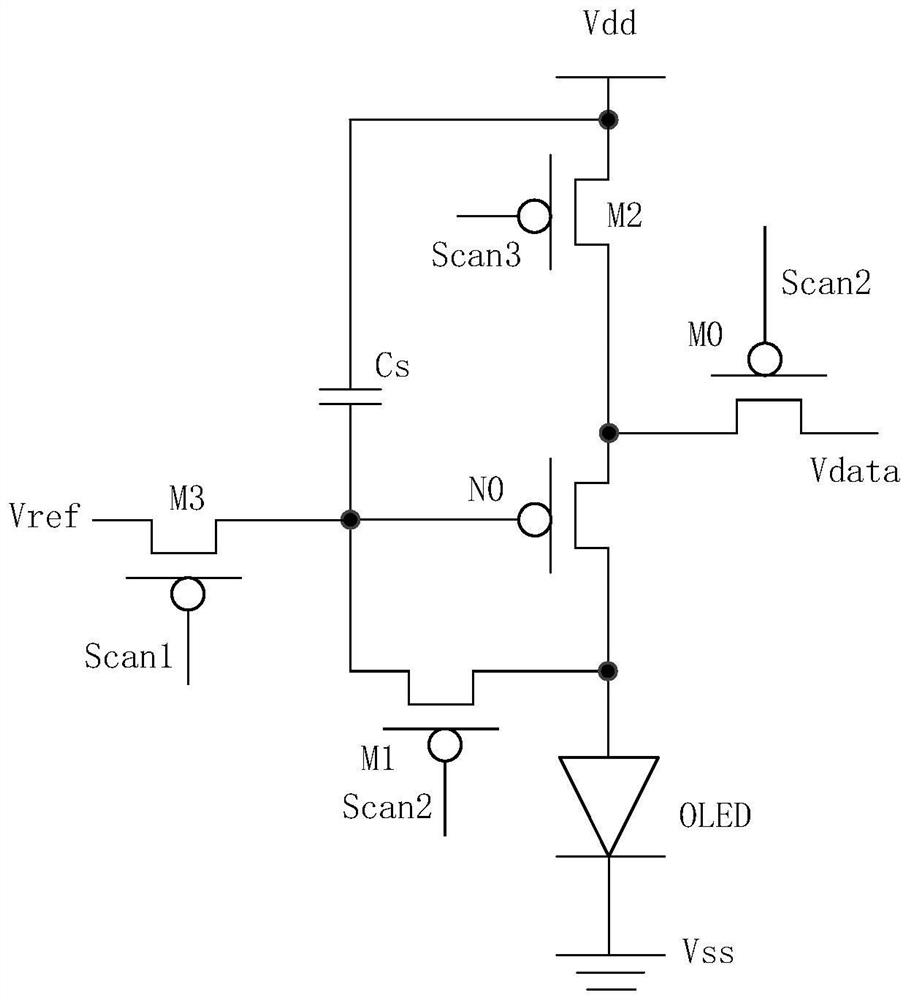
[0047] figure 1 A schematic structural diagram of a pixel driving circuit provided in the prior art. Such as figure 1As shown, the pixel driving circuit includes a switching transistor M0, a compensation transistor M1, a light emission control transistor M2, an initialization transistor M3, a driving transistor N0 and a storage capacitor Cs. The gate of the initialization transistor M3 is connected to the first scan line Scan1 to receive the first scan signal, the source is connected to the initialization signal...


PUM


Abstract

The invention discloses an array substrate, a manufacturing method of the array substrate and a display panel. The array substrate comprises: a substrate; the pixel driving circuit is arranged on the substrate, the pixel driving circuit comprises a driving transistor and a first transistor, the first transistor is located on a grid leakage path of the driving transistor, and the threshold voltage of the first transistor is larger than that of the driving transistor. The threshold voltage of the first transistor is set to be greater than the threshold voltage of the driving transistor, so that the leakage current of the first transistor in a turn-off state is relatively small, the leakage current on a grid leakage path of the driving transistor where the first transistor is located can be reduced, the grid potential holding time of the driving transistor is prolonged, and the driving efficiency is improved. Therefore, the driving current formed by the driving transistor is relatively stable, the flicker phenomenon of the display panel is reduced, and the display image quality of the display panel is improved.

Description

technical field [0001] Embodiments of the present invention relate to the technical field of display, and in particular, to an array substrate, a method for manufacturing the array substrate, and a display panel. Background technique [0002] Active-matrix organic light emitting diode (AMOLED) display panels have been widely used in the display field because they are superior to liquid crystal display panels in terms of display color saturation, power consumption, and bending. During the display process of the AMOLED display panel, the pixel driving circuit drives the light emitting device to emit light. In the prior art, the pixel driving circuit includes a driving transistor, and the gate of the driving transistor has a leakage current phenomenon, and the stability is relatively poor, resulting in unstable luminance of the light emitting device, thereby affecting the display quality of the AMOLED display panel. Contents of the invention [0003] The invention provides a...

Claims


Application Information

Patent Timeline
IPC IPC(8): G09G3/3225G09G3/3233
CPCG09G3/3225G09G3/3233
Inventor 陈发祥马应海刘雪郭双郭子栋
Owner YUNGU GUAN TECH CO LTD
Why Eureka
Try Eureka