Testing device and testing method for high-precision analog-to-digital conversion chip

A test device and analog-to-digital conversion technology, which is applied in the direction of analog/digital conversion calibration/test, analog/digital conversion, code conversion, etc., can solve the problems that the test accuracy cannot meet the chip test requirements, and the unfavorable chip stable mass production, etc., to achieve Improve test efficiency, achieve test results, and save reading time

Pending Publication Date: 2022-03-08
SG MICRO
View PDF0 Cites 0 Cited by
  • Summary
  • Abstract
  • Description
  • Claims
  • Application Information

AI Technical Summary

Problems solved by technology

Since the test accuracy of the high-precision boards of the existing test machines cannot meet the chip test requirements with higher and higher precision requirements, and the existing measurement is also greatly affected by the environment, which is not conducive to the stable mass production of chips

Method used


Image

  • Testing device and testing method for high-precision analog-to-digital conversion chip
  • Testing device and testing method for high-precision analog-to-digital conversion chip

Examples


Embodiment Construction

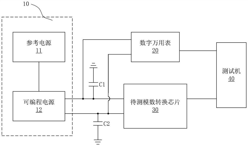
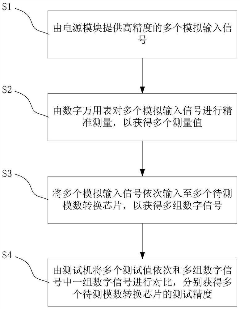
[0027] In order to facilitate the understanding of the present invention, the present invention will be described more fully below with reference to the associated drawings. Preferred embodiments of the invention are shown in the accompanying drawings. However, the present invention can be implemented in different forms and is not limited to the embodiments described herein. On the contrary, these embodiments are provided to make the understanding of the disclosure of the present invention more thorough and comprehensive.

[0028] Unless otherwise defined, all technical and scientific terms used herein have the same meaning as commonly understood by one of ordinary skill in the technical field of the invention. The terms used herein in the description of the present invention are for the purpose of describing specific embodiments only, and are not intended to limit the present invention.

[0029] Hereinafter, the present invention will be described in detail with reference t...


PUM


Abstract

The invention discloses a high-precision analog-to-digital conversion chip testing device and method, and the device comprises a power module which is used for providing a plurality of high-precision analog input signals which are converted into a plurality of groups of digital signals after passing through a plurality of analog-to-digital conversion chips to be tested; the digital multimeter is connected with the input end of the analog-to-digital conversion chip to be measured and is used for accurately measuring the analog input signals so as to obtain a plurality of corresponding measured values; and the test machine is used for comparing the plurality of test values with one group of digital signals in the plurality of groups of digital signals in sequence so as to respectively obtain the test precision of the plurality of analog-to-digital conversion chips to be tested, and each group of digital signals correspondingly comprises a plurality of digital signals. According to the invention, high-precision and high-efficiency testing of the to-be-tested analog-to-digital conversion chip is realized, and stable mass production testing of the to-be-tested analog-to-digital conversion chip is realized.

Description

technical field [0001] The invention relates to the technical field of chip testing, in particular to a testing device and testing method for a high-precision analog-to-digital conversion chip. Background technique [0002] The performance parameters of the ADC chip (Analog-to-Digital Converter, analog-to-digital converter) need to be tested by a testing machine. During the test, a DC power supply on the testing machine is connected to the ADC chip to provide reference power for the ADC chip. The testing machine provides analog input signals and clock signals for the ADC chip. After the analog input signal passes through the ADC chip, it is converted into a digital signal, and the The digital signal is output to a digital processor on the ATE. Simultaneously, the analog input signal measurement and acquisition of the ADC chip is realized through the testing machine. [0003] In the existing testing process of the ADC chip, the high-precision board on the testing machine is...

Claims


Application Information

Patent Timeline
Patent Type & Authority Applications(China)
IPC IPC(8): H03M1/10
CPCH03M1/1071
Inventor 邴春秋
Owner SG MICRO
Why Eureka
Try Eureka