Supercharge Your Innovation With Domain-Expert AI Agents!

Method for positioning wafer in edge etching chamber

A positioning method and etching cavity technology, which are used in electrical components, semiconductor/solid-state device manufacturing, circuits, etc., can solve problems such as position deviation, affect product quality, and reduce process accuracy, so as to ensure etching accuracy and improve product quality. , to ensure the effect of transmission accuracy

Pending Publication Date: 2022-03-08
BEIJING NAURA MICROELECTRONICS EQUIP CO LTD
View PDF0 Cites 0 Cited by
  • Summary
  • Abstract
  • Description
  • Claims
  • Application Information

AI Technical Summary

Problems solved by technology

[0004] The purpose of the embodiment of the present application is to provide a positioning method for positioning a wafer in an edge etching chamber, which can solve the problem that the position deviation of the wafer in the edge etching chamber reduces the process accuracy and affects the product quality

Method used


Image

  • Method for positioning wafer in edge etching chamber
  • Method for positioning wafer in edge etching chamber
  • Method for positioning wafer in edge etching chamber

Examples


Embodiment Construction

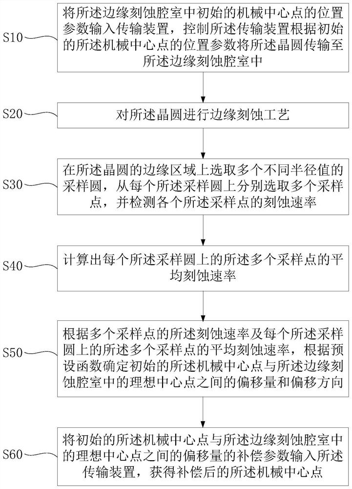
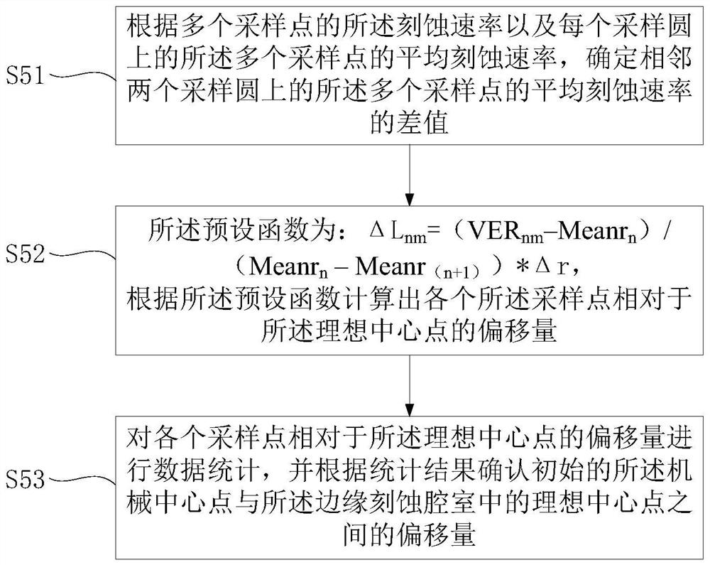
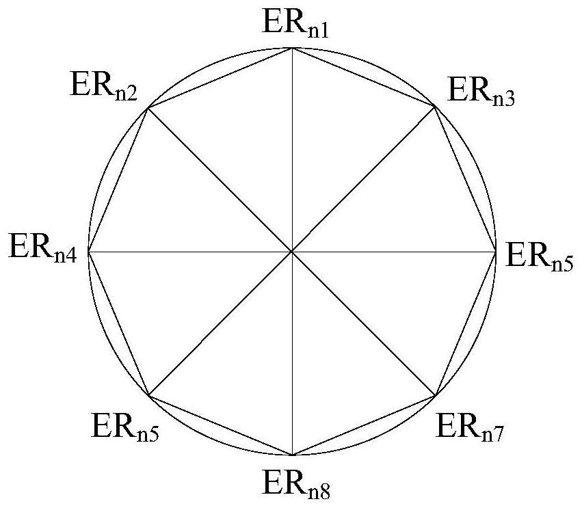
[0017] The following will clearly and completely describe the technical solutions in the embodiments of the present application with reference to the drawings in the embodiments of the present application. Obviously, the described embodiments are part of the embodiments of the present application, not all of them. Based on the embodiments in this application, all other embodiments obtained by persons of ordinary skill in the art without creative efforts fall within the protection scope of this application.

[0018] The terms "first", "second" and the like in the specification and claims of the present application are used to distinguish similar objects, and are not used to describe a specific sequence or sequence. It should be understood that the terms so used are interchangeable under appropriate circumstances such that the embodiments of the application can be practiced in sequences other than those illustrated or described herein, and that references to "first," "second," et...


PUM

PropertyMeasurementUnit
Radiusaaaaaaaaaa

Abstract

The invention discloses a positioning method for positioning a wafer in an edge etching chamber, and relates to the field of semiconductor processes. The positioning method comprises the following steps: inputting a position parameter of an initial mechanical center point in an edge etching chamber into a transmission device, and controlling the transmission device to transmit a wafer into the edge etching chamber according to the position parameter; carrying out an edge etching process on the wafer; selecting a plurality of sampling circles with different radius values on the edge area of the wafer; selecting a plurality of sampling points from each sampling circle, and detecting the etching rate of each sampling point; calculating the average etching rate of a plurality of sampling points on each sampling circle; determining an offset and an offset direction between the initial mechanical center point and an ideal center point in the edge etching chamber according to a preset function; and inputting the compensation parameter of the offset into a transmission device to obtain a compensated mechanical center point. The problems that the process precision is reduced and the product quality is influenced due to position deviation of the wafer in the edge etching chamber can be solved.

Description

technical field [0001] The application belongs to the technical field of semiconductor technology, and in particular relates to a positioning method for positioning a wafer in an edge etching chamber. Background technique [0002] Semiconductor equipment processes wafers through physical and chemical means, and some processing processes need to be realized in a certain vacuum environment. The module that realizes the processing process is called a process module. During the process of the wafer entering the vacuum environment from the atmospheric environment, it needs to be realized through the transmission system. Among them, the transmission system includes a manipulator, a transition chamber, a vacuum chamber, and the like. [0003] During the transfer process of the wafer, the manipulator in the atmosphere places the wafer in the transition chamber, and the manipulator in the vacuum chamber transfers the wafer from the transition chamber to the chamber of the process mo...

Claims


Application Information

Patent Timeline
IPC IPC(8): H01L21/68H01L21/67
CPCH01L21/68H01L21/67213
Inventor 王炳元王松涛张德群李尔林
Owner BEIJING NAURA MICROELECTRONICS EQUIP CO LTD
Features
  • R&D
  • Intellectual Property
  • Life Sciences
  • Materials
  • Tech Scout
  • Unparalleled Data Quality
  • Higher Quality Content
  • 60% Fewer Hallucinations
Learn More