
Pure-phase high-resolution spatial light modulator with 4 pi modulation range

A spatial light modulator, high-resolution technology, applied in the field of micro-nano optics, which can solve the problems of shrinking pixel unit size, increasing device volume and weight, unfavorable to the development of ultra-thin, miniaturization and integration of active optical devices. , to achieve the effect of reducing vertical size, high resolution, and large imaging field of view

Pending Publication Date: 2022-03-04
WUHAN UNIV
View PDF0 Cites 2 Cited by
  • Summary
  • Abstract
  • Description
  • Claims
  • Application Information

AI Technical Summary

Problems solved by technology

In order to provide a sufficient 2π phase modulation range, the liquid crystal spatial light modulator often needs a certain thickness. If it is necessary to achieve a phase depth modulation greater than 2π, the longitudinal dimension of the device will be further expanded, which not only increases the volume and weight of the device, but also It limits the further reduction of the pixel unit size, which is not conducive to the development of active optical devices towards ultra-thin, miniaturized and integrated

Method used


Image

  • Pure-phase high-resolution spatial light modulator with 4 pi modulation range
  • Pure-phase high-resolution spatial light modulator with 4 pi modulation range
  • Pure-phase high-resolution spatial light modulator with 4 pi modulation range

Examples


Embodiment 1

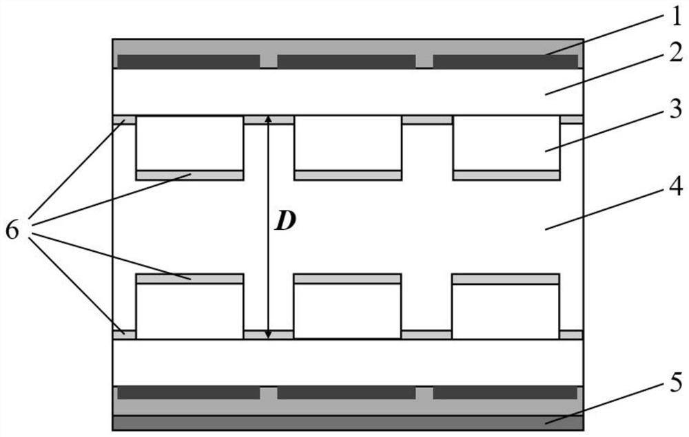
[0031] In this example, figure 1 It is a schematic diagram of the overall structure of a phase-only high-resolution spatial light modulator with a 4π modulation range, including: an electrode layer 1, two metasurfaces (composed of a substrate 2 and a nano-unit structure 3), a liquid crystal medium 4, and a reflective layer 5 and alignment layer 6. The total thickness of the liquid crystal layer is D.

[0032] In this embodiment, the device works in the near-infrared band, the incident light is linearly polarized light, and the working wavelength is 1282 nm.

[0033] In this embodiment, the material of the liquid crystal layer is selected from E7 nematic liquid crystal, and the refractive index variation range is n LC =1.7~1.51, the thickness D is taken as 1720nm.

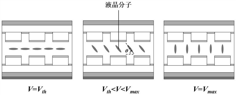
[0034] In this embodiment, the initial state of the liquid crystal molecules determined by the alignment layer is horizontal, such as figure 2 As shown, that is, the initial refractive index of the liquid cryst...


PUM

PropertyMeasurementUnit
refractive indexaaaaaaaaaa

Abstract

The invention discloses a pure-phase high-resolution spatial light modulator in a 4-pi modulation range. The pure-phase high-resolution spatial light modulator mainly comprises two resonance type metasurfaces, a liquid crystal medium environment, an electrode layer, a reflecting layer and the like, wherein the resonance type metasurfaces are oppositely arranged and are composed of dielectric medium sub-wavelength unit structures and substrates. Based on the characteristic that the resonance spectrum of the metasurface can be adjusted by changing electromagnetic parameters of an external environment, the Huygens metasurface is combined with liquid crystal, and light wave phase point-by-point continuous dynamic modulation under the sub-wavelength pixel scale is achieved. In addition, due to the design of introducing the laminated metasurface and the reflecting layer, the total phase modulation depth can reach 4 pi, and extremely high working efficiency can be kept. Compared with the existing pure-phase spatial light modulator technology, the device provided by the invention effectively improves the resolution and dynamic range of the device, is wider in application scene, is smaller in size, is lighter in weight, and is easier to integrate.

Description

technical field [0001] The invention relates to the field of micro-nano optics technology, in particular to a 4π modulation range pure phase high-resolution spatial light modulator. Background technique [0002] The phase modulation of the incident light wave by the traditional liquid crystal spatial light modulator is mostly based on the phase accumulation of the light wave in a medium with a certain thickness. When the refractive index of the liquid crystal is changed by applying an external voltage, the phase of the beam accumulation will change accordingly, achieving dynamic adjustment. Effect. In order to provide a sufficient 2π phase modulation range, the liquid crystal spatial light modulator often needs a certain thickness. If it is necessary to achieve a phase depth modulation greater than 2π, the longitudinal dimension of the device will be further expanded, which not only increases the volume and weight of the device, but also This limits the further reduction of...

Claims


Application Information

Patent Timeline
Patent Type & Authority Applications(China)
IPC IPC(8): G02F1/139G02F1/1335
CPCG02F1/1393G02F1/1335
Inventor 彭畅郑国兴李子乐
Owner WUHAN UNIV
Learn More