Screen defect classification method, electronic equipment and storage medium
A defect classification and defect type technology, used in instruments, character and pattern recognition, computer parts and other directions, can solve the problems of large image area span, increased maintenance workload, low screen defect classification accuracy, etc., to improve the classification accuracy. rate effect
- Summary
- Abstract
- Description
- Claims
- Application Information
AI Technical Summary
Problems solved by technology
Method used
Image
Examples
Embodiment 1
[0060] Traditional image processing algorithms need to adjust parameters and operation steps according to different defect types, which increases the workload of maintenance. However, when the convolutional neural network algorithm acquires image defect ROI areas, when the defect ROI area has a large span, it may lead to the collection of defects. The incomplete ROI area will reduce the classification accuracy of the screen defect detection network.
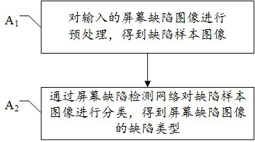
[0061] For the above problems, the embodiment of this application provides a solution, please refer to figure 1 , figure 1 It is a schematic flowchart of defect classification of screen defect images shown in the embodiment of the present application.
[0062] The screen defect image is preprocessed to obtain a defect sample image, and the defect sample image is input into the screen defect detection network for classification, and the defect type of the screen defect image is obtained.
[0063] The defect classification proces...
Embodiment 2
[0083] In order to enhance the generalization ability of the screen defect detection network and improve the classification accuracy of the screen defect detection network.
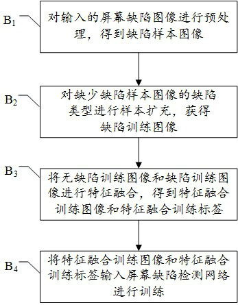
[0084] The embodiment of this application provides a training method for the screen defect detection network, please refer to figure 2 , figure 2 It is a schematic flowchart of the training method of the screen defect detection network shown in the embodiment of the present application.
[0085] B1. Preprocessing the input screen defect image to obtain a defect sample image.
[0086] In the embodiment of the present application, the content of step B1 is the same as that of step A1 in the first embodiment above, and will not be repeated here.
[0087] B2. Carrying out sample expansion for defect types lacking defect sample images to obtain defect training images.
[0088] Exemplary: performing one or more of rotation, translation, mirroring, and random cropping on a small number of defect sample imag...
Embodiment 3
[0112] After the defect sample images are classified through the screen defect detection network and the defect types of the screen defect images are obtained, it is necessary to improve the classification accuracy of defect types with low classification accuracy and optimize the screen defect detection network.
[0113] The embodiment of this application provides a method for optimizing the screen defect detection network, please refer to Figure 4 , Figure 4 It is a schematic flowchart of an optimized screen defect detection network shown in the embodiment of the present application.
[0114] C1. Add defect training images corresponding to defect types with low classification accuracy.
[0115] For example, if the defect sample images are classified by the screen defect detection network and it is found that the classification accuracy of the screen defects of the white point-like uneven brightness type is low, correspondingly, the defect training images of the white point...
PUM
 Abstract
Description
Claims
Application Information
 - R&D
- Intellectual Property
- Life Sciences
- Materials
- Tech Scout
- Unparalleled Data Quality
- Higher Quality Content
- 60% Fewer Hallucinations
Browse by: Latest US Patents, China's latest patents, Technical Efficacy Thesaurus, Application Domain, Technology Topic, Popular Technical Reports.
© 2025 PatSnap. All rights reserved.Legal|Privacy policy|Modern Slavery Act Transparency Statement|Sitemap|About US| Contact US: help@patsnap.com


