Semiconductor Automatic Partitioning Method Based on Panoramic Segmentation

An automatic partitioning and semiconductor technology, applied in reasoning methods, image analysis, image enhancement, etc., can solve the problems of weak structural adaptability, cumbersome parameter adjustment of partitioning scheme, etc., achieving strong structural versatility, eliminating the need for human-computer interaction, Solve the tedious effect of parameter adjustment

Active Publication Date: 2022-04-12
聚时科技(江苏)有限公司
View PDF13 Cites 0 Cited by
  • Summary
  • Abstract
  • Description
  • Claims
  • Application Information

AI Technical Summary

Problems solved by technology

[0008] The purpose of the present invention is to provide a semiconductor automatic partitioning method based on panoramic segmentation, which can solve the problems of cumbersome parameter adjustment, weak structural adaptability, and time-consuming partitioning in traditional partitioning schemes.

Method used


Image

  • Semiconductor Automatic Partitioning Method Based on Panoramic Segmentation
  • Semiconductor Automatic Partitioning Method Based on Panoramic Segmentation
  • Semiconductor Automatic Partitioning Method Based on Panoramic Segmentation

Examples


Embodiment Construction

[0047] The technical solutions in the embodiments of the present invention will be clearly and completely described below in conjunction with specific embodiments. Apparently, the described embodiments are only some of the embodiments of the present invention, but not all of them. Based on the embodiments of the present invention, all other embodiments obtained by persons of ordinary skill in the art without making creative efforts belong to the protection scope of the present invention.

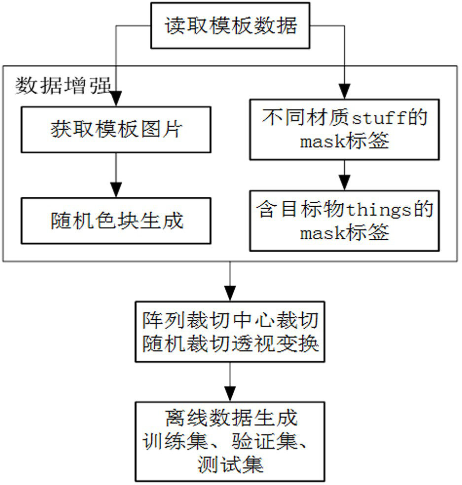
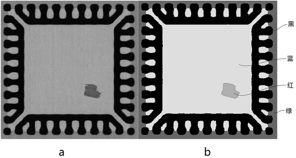
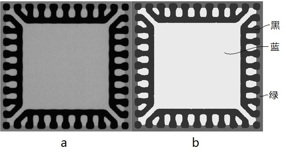
[0048] The zoning modeling process is a key step in the AOI semiconductor defect detection modeling process. The quality of the zoning results directly affects the accuracy of subsequent defect detection. This scheme proposes an automatic semiconductor partitioning method based on panoramic segmentation, which can solve the problems of cumbersome parameter adjustment, weak structural adaptability, and time-consuming partitioning in traditional partitioning schemes. This solution can include...


PUM


Abstract

The invention belongs to the technical field of semiconductor defect detection and image processing, and specifically relates to a semiconductor automatic partition method based on panoramic segmentation. The method is based on a panoramic segmentation network. First, template data of several products are collected as training data for the panoramic segmentation network. The template data includes Template picture and mask picture; define the material in the mask picture as stuff, generate random-sized color blocks at any position on the template picture, and map the color blocks to the mask picture to define things; secondly, use the training data to train the panorama segmentation network, Get a panoramic segmentation network that can model automatic partitioning of semiconductors. The partition template can be obtained by inputting the partitioned picture into the panoramic segmentation network. This method can solve the problems of cumbersome parameter adjustment, weak structural adaptability, and time-consuming partitioning in traditional partitioning schemes.

Description

technical field [0001] The invention belongs to the technical field of semiconductor defect detection and image processing, and in particular relates to a semiconductor automatic partition method based on panorama segmentation. Background technique [0002] With the rise of the Internet of Things, 5G industry, and smart wearable devices, the semiconductor industry has ushered in rapid development under the blessing of industrial policies, and the market demand has expanded dramatically. However, the semiconductor manufacturing industry needs to solve many problems in terms of production speed and production quality, among which defect detection is one of the important processes in the semiconductor manufacturing process. At present, most semiconductor manufacturers use manual quality inspection to detect defects. Different processes require experienced operators to concentrate on detecting defects with naked eyes. This manual quality inspection method is time-consuming, ine...

Claims


Application Information

Patent Timeline
Patent Type & Authority Patents(China)
IPC IPC(8): G06T7/11G06T7/12G06T7/13G06T7/187G06T5/00G06T1/20G06N5/04
CPCG06T7/11G06T7/12G06T7/13G06T7/187G06T5/00G06T1/20G06N5/04G06T2207/20081G06T2207/20084G06T2207/30148G06T2207/20021
Inventor 糜泽阳张记霞郑军
Owner 聚时科技(江苏)有限公司
Why Eureka
Try Eureka