Photoelectric device based on ferroelectric PN junction, and preparation method thereof

A technology of optoelectronic devices and PN junctions, applied in electrical components, semiconductor devices, circuits, etc., and can solve the problems of low efficiency of optoelectronic devices

Pending Publication Date: 2021-12-14
THE NAT CENT FOR NANOSCI & TECH NCNST OF CHINA
View PDF0 Cites 1 Cited by
  • Summary
  • Abstract
  • Description
  • Claims
  • Application Information

AI Technical Summary

Problems solved by technology

[0006] The purpose of the present invention is to provide a ferroelectric PN junction-based photoelectric device and its preparation method to solve the problem of low efficiency of photoelectric devices in the prior art

Method used


Image

  • Photoelectric device based on ferroelectric PN junction, and preparation method thereof
  • Photoelectric device based on ferroelectric PN junction, and preparation method thereof
  • Photoelectric device based on ferroelectric PN junction, and preparation method thereof

Examples


Embodiment Construction

[0034] The following examples are used to illustrate the present invention, but are not intended to limit the scope of the present invention.

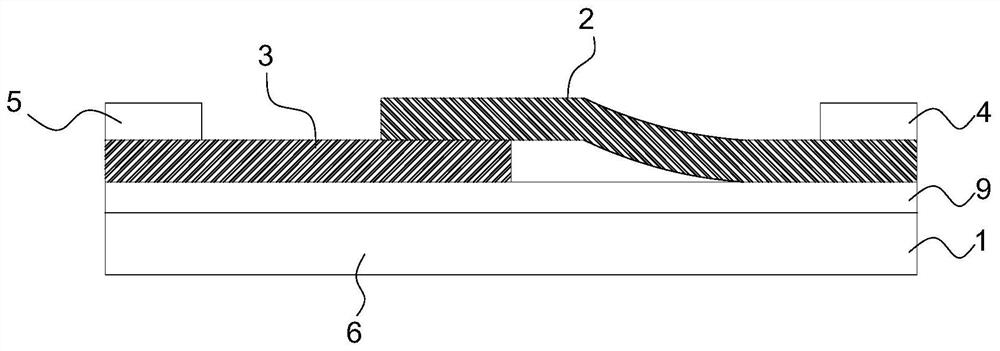
[0035] The present invention provides a photoelectric device based on a ferroelectric PN junction, comprising a substrate 1; a ferroelectric semiconductor material layer 2 and a photosensitive material layer 3 forming a PN junction on the substrate 1, wherein the ferroelectric semiconductor material layer 2 and Partially overlap with the photosensitive material layer 3 in the vertical direction and form a PN junction on the contact surface; the first electrode 4 and the second electrode 5 are respectively connected to the ferroelectric semiconductor material layer 2 and the photosensitive material layer 3 electrical connection.

[0036] Specifically, the substrate 1 is located at the bottom of the ferroelectric semiconductor material layer 2 and the photosensitive material layer 3 and plays a supporting role. The substrate 1 is made o...


PUM

PropertyMeasurementUnit
thicknessaaaaaaaaaa

Abstract

The invention relates to a photoelectric device based on ferroelectric PN junction, and a preparation method thereof. The photoelectric device comprises: a substrate; a ferroelectric semiconductor material layer and a photosensitive material layer which are located on the substrate to form the PN junction, wherein the ferroelectric semiconductor material layer and the photosensitive material layer are partially overlapped in the vertical direction, and the PN junction is formed on the contact face of the ferroelectric semiconductor material layer and the photosensitive material layer; and a first electrode and a second electrode which are electrically connected with the ferroelectric semiconductor material layer and the photosensitive material layer respectively. The built-in potential can be formed after the ferroelectric semiconductor material and the photosensitive material in the PN junction are in contact, and after the grid voltage pulse is applied, the built-in potential can be regulated and controlled in a non-volatile manner, so that the short-circuit current of the device under illumination is regulated and controlled in a non-volatile manner, and the efficiency of the photoelectric device is further improved.

Description

[0001] This application claims the priority of the previous patent application filed on August 5, 2021 with the application number "202110896408.1" and the application title "An optoelectronic device and its preparation method". technical field [0002] The invention relates to the technical field of inorganic semiconductor nanometer materials, in particular to a photoelectric device based on a ferroelectric PN junction and a preparation method thereof. Background technique [0003] The photoelectric effect refers to the phenomenon that when light shines on the metal surface, electrons in the metal can escape from the surface. Optoelectronic devices refer to devices made according to the photoelectric effect called optoelectronic devices, also known as photosensitive devices. [0004] Common optoelectronic devices usually include photocells, photodiodes, and phototriodes. Their working principle is that when light is irradiated on the optoelectronic device, the electrical pr...

Claims


Application Information

Patent Timeline
Patent Type & Authority Applications(China)
IPC IPC(8): H01L31/109H01L31/113H01L31/032H01L31/18
CPCH01L31/109H01L31/113H01L31/032H01L31/18
Inventor 王振兴王艳荣王峰何军
Owner THE NAT CENT FOR NANOSCI & TECH NCNST OF CHINA
Why Eureka
Try Eureka