Display panel, manufacturing method thereof and display device

A technology for display panels and manufacturing methods, applied in the fields of nonlinear optics, instruments, optics, etc., can solve problems affecting display panel display effects, short circuits, test traces with electrification, etc., so as to improve display effects and avoid contact short circuits , the effect of reducing the possibility of short-circuit problems

Active Publication Date: 2021-12-07
HKC CORP LTD
View PDF4 Cites 1 Cited by
  • Summary
  • Abstract
  • Description
  • Claims
  • Application Information

AI Technical Summary

Problems solved by technology

[0003] Generally speaking, the liquid crystal display panel is formed after cutting the display motherboard. Therefore, the test traces on the display motherboard will also be cut, so that they are exposed to the air from the side of the liquid crystal display panel. When the internal circuit is directly or indirectly connected to the test wiring, the exposed test wiring is electrically charged, which may cause a short circuit problem due to contact with the external ground terminal, thereby affecting the display effect of the display panel.

Method used


Image

  • Display panel, manufacturing method thereof and display device
  • Display panel, manufacturing method thereof and display device
  • Display panel, manufacturing method thereof and display device

Examples


Embodiment 1

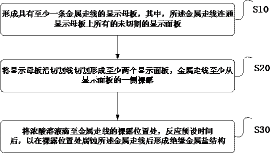
[0050] like figure 1 As shown, as the first embodiment of the present application, a method for manufacturing a display panel is disclosed, including steps:

[0051] S10: forming a display motherboard with at least one metal trace, wherein the metal trace communicates with all uncut display panels on the display motherboard;

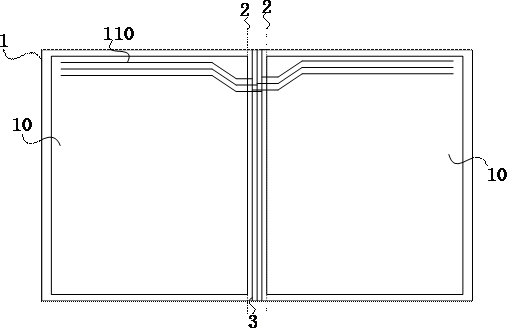
[0052] S20: cutting the display motherboard along the cutting line to form at least two display panels, and the metal traces are exposed on at least one side of the display panels;

[0053] S30: drop the concentrated acid solution onto the bare position of the metal trace, and react for a preset time, so as to form an insulating metal salt structure after corroding the metal trace at the bare position.

[0054] In this application, the concentrated acid solution and the bare position of the metal wiring are subjected to oxidation-reduction reaction to generate the corresponding insulating metal salt structure, that is, the metal wiring of the insulating...

Embodiment 2

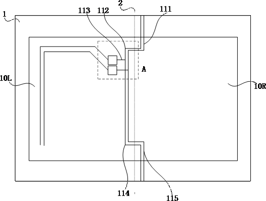
[0087] Specifically, there are many options for the location of corrosion: such as Figure 8 As shown, as the second embodiment of the present application, another method for manufacturing a display panel is disclosed, including steps:

[0088] S10: forming a display motherboard with at least one metal trace, wherein the metal trace communicates with all uncut display panels on the display motherboard;

[0089] S20: cutting the display motherboard along the cutting line to form at least two display panels, and the metal traces are exposed on at least one side of the display panels;

[0090] S32: directly dripping the concentrated acid solution to the exposed area corresponding to the metal wiring on the side of the display panel;

[0091] S40: Perform a cleaning step after a preset time.

[0092] Corresponding to this embodiment, a display panel is disclosed. The display panel includes: a first substrate, at least one metal wiring and an insulating layer, the metal wiring is...

Embodiment 3

[0095] like Figure 9 As shown, as the third embodiment of the present application, the present application also discloses a display device, the display device 400 includes a conductive tape 420, a circuit board 410 and the above-mentioned display panel 10, and the conductive tape 420 corresponds to the display panel 10, the circuit board 410 is bound on the display panel. The conductive tape in this embodiment can be directly attached to the side of the display panel, and the exposed positions corresponding to the metal traces can be directly in contact with the metal traces without short circuit.


PUM


Abstract

The invention discloses a test circuit of a display panel and a display device. The test circuit comprises a plurality of test wires, a plurality of first active switches and a protection circuit, wherein the test wires comprise a high level signal test wire, a low level signal test wire and at least one test signal wire; the first active switch controls the on and off of the test signal line, the low-level signal test line and the high-level signal test line; the high-level signal test line is also connected with the control end of each first active switch; the protection circuit comprises a control signal input end and a control signal output end, the control signal input end is connected with the high-level signal wire and the low-level signal wire, and the control signal output end is connected with the control end of each first active switch; when the display panel works normally, the protection circuit receives a low-level signal on the low-level signal line and outputs a control signal to control the first active switch to be turned off. According to the scheme, the problem of short circuit of test wiring is solved.

Description

technical field [0001] The present application relates to the field of display technology, and in particular to a display panel, a manufacturing method thereof, and a display device. Background technique [0002] A liquid crystal display generally includes a liquid crystal display panel, a backlight module, an optical film, a plastic frame, and conductive adhesive tape arranged on the side of the display panel. [0003] Generally speaking, the liquid crystal display panel is formed after cutting the display motherboard. Therefore, the test traces on the display motherboard will also be cut, so that they are exposed to the air from the side of the liquid crystal display panel. At this time, because the internal circuit is directly or indirectly connected to the test wiring, the exposed test wiring is electrically charged, and may contact the external ground terminal to cause a short circuit problem, thereby affecting the display effect of the display panel. Contents of the ...

Claims


Application Information

Patent Timeline
Patent Type & Authority Applications(China)
IPC IPC(8): G02F1/13G02F1/1333
CPCG02F1/1303G02F1/133351G02F1/136254G02F2201/50G02F1/1316G02F1/133345G02F1/133514G02F1/1339G02F1/13452
Inventor 杨维世许益祯王立苗任春晖唐榕赵聪聪袁海江
Owner HKC CORP LTD
Why Eureka
Try Eureka