


Quick Research
Generate reliable direction feasibility study reports for your R&D in just a few steps.

Technical Q&A
Discover and master advanced knowledge NOW. Basics, ideas, possibilities, all at once.

Find Solutions
As an expert in R&D theories, this can generate solutions to your technical problems instantly.

Evaluate Feasibility
Analyze your overall solution with one click, know your potential R&D risks in advance.

Monitor Landscape
Get weekly tech updates, stay abreast of the latest tech innovations and key insights.
Transparent display panel, preparation method thereof and display device
A transparent display panel and display substrate technology, which is applied in semiconductor/solid-state device manufacturing, organic semiconductor devices, semiconductor devices, etc., can solve the problem of low color purity and achieve the effect of improving color purity
- Summary
- Abstract
- Description
- Claims
- Application Information
AI Technical Summary
Problems solved by technology
Method used
Image

Examples
Embodiment 1
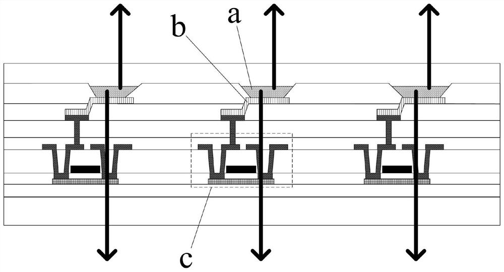
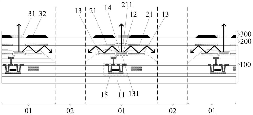
[0054] figure 2 A cross-sectional view of a transparent display panel according to Embodiment 1 of the present invention is shown, refer to figure 2 , the transparent display panel includes a stacked display substrate 100 and a touch substrate 200 , the transparent display panel is divided into a pixel area 01 and a transparent area 02 located between the pixel areas 01 , and the pixel unit is set in the pixel area 01 .
[0055] refer to figure 2 , the display substrate 100 includes a substrate 11, and an anode layer 12 located in the pixel area 01, a first electrode layer 13, and a light-emitting functional layer 14; the first electrode layer 13 and the anode layer 12 are arranged separately on the same layer, that is, arranged on the same layer The first electrode layer 13 and the anode layer 12 are not electrically connected to each other, the anode layer 12 and the first electrode layer 13 have high reflectivity, and the orthographic projection of the first electrode l...
Embodiment 2
[0106] refer to Figure 8 , which shows a flow chart of the steps of a method for manufacturing a transparent display panel according to Embodiment 2 of the present invention, the method includes the following steps:
[0107] Step 801: Form an anode layer and a first electrode layer on the same layer on the substrate; the substrate includes a substrate, the first electrode layer and the anode layer are located in the pixel area, the first electrode layer and the anode layer are separately arranged, and the anode layer and the first electrode layer Has high reflectivity.
[0108] Among them, a substrate 11 can be provided first, and then a thin film transistor 15 and a capacitor structure 16 are prepared in the pixel region 01 on the substrate 11. The thin film transistor 15 includes a first wiring layer 17. For details, refer to related technologies, as follows: Figure 9 The transparent display panel shown. Then, a film layer of the first planar layer can be formed, and pat...
Embodiment 3
[0126] The embodiment of the present invention also discloses a display device, including the above-mentioned transparent display panel.
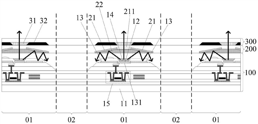
[0127] In the embodiment of the present invention, the first electrode layer with high reflectivity in the display substrate and the second electrode layer with high reflectivity in the touch substrate can be used to form a light guide structure, and the small-angle light emitted by the light-emitting functional layer can pass through the The first hollow area surrounded by the second electrode layer exits from the pixel area on the side close to the touch substrate, and the large-angle light emitted by the light-emitting functional layer enters the light-guiding structure and is reflected by the light-guiding structure at least once , guided to the transparent area near the side of the display substrate to emit, thereby realizing double-sided display. In the embodiment of the present invention, the anode layer still has a high reflectivity...
PUM
| Property | Measurement | Unit |
|---|---|---|
| angle | aaaaa | aaaaa |
| length | aaaaa | aaaaa |
Abstract
Description
Claims
Application Information
 - R&D Engineer
- R&D Manager
- IP Professional
- Industry Leading Data Capabilities
- Powerful AI technology
- Patent DNA Extraction
Browse by: Latest US Patents, China's latest patents, Technical Efficacy Thesaurus, Application Domain, Technology Topic, Popular Technical Reports.
© 2024 PatSnap. All rights reserved.Legal|Privacy policy|Modern Slavery Act Transparency Statement|Sitemap|About US| Contact US: help@patsnap.com