
Display substrate, preparation method thereof and display device

A display substrate and display area technology, applied in semiconductor/solid-state device manufacturing, electrical components, electric solid-state devices, etc., can solve the problems of occupying a large area, poor anti-crack extension effect, unfavorable narrow frame, etc., to prevent cracking , Improve the effect of poor water vapor intrusion and ensure a flat trend

Pending Publication Date: 2021-10-26
BOE TECH GRP CO LTD +1
View PDF0 Cites 1 Cited by
  • Summary
  • Abstract
  • Description
  • Claims
  • Application Information

AI Technical Summary

Problems solved by technology

However, this kind of Crack DAM structure is not effective in anti-crack extension. At the same time, the gap and Crack DAM structure will occupy a large area, which is not conducive to the realization of narrow borders.

Method used


Image

  • Display substrate, preparation method thereof and display device
  • Display substrate, preparation method thereof and display device
  • Display substrate, preparation method thereof and display device

Examples


preparation example Construction

[0108] In some embodiments, the preparation method also includes:

[0109] Step S201, forming a touch layer on the side of the film layer unit away from the substrate;

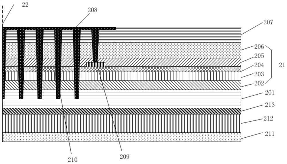
[0110] Step S202 , forming a second protection layer on a side of the touch layer away from the substrate. Wherein, the second protective layer 207 is used to protect the touch layer and prevent the touch layer from being damaged.

[0111] In some embodiments, the first protection layer is located in the edge protection area; the second protection layer includes a first sub-protection area located in the edge protection area and a second sub-protection area located in the display area The first sub-protection area is disposed between the film layer unit and the first protection layer, and the end of the dam structure away from the base penetrates through the first sub-protection area. The thickness of the first protective layer is less than 1 μm.

[0112] In this embodiment, before step S103 , a touch layer...


PUM

PropertyMeasurementUnit
thicknessaaaaaaaaaa

Abstract

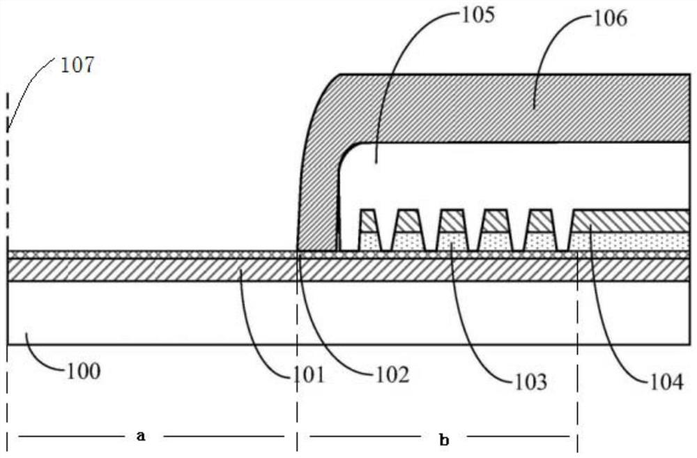
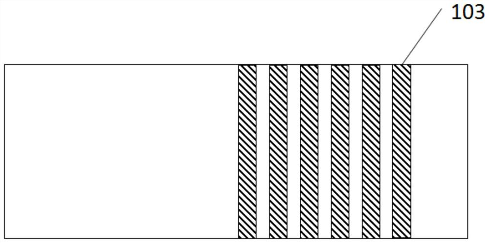
The invention provides a display substrate, a preparation method thereof and a display device. The display substrate comprises a display area and an edge protection area arranged on the periphery of the display area. The display substrate further comprises a substrate; a film layer unit which is arranged on the substrate and comprises a plurality of organic layers and / or inorganic layers which are arranged in a stacked mode, wherein the orthographic projection of the film layer unit on the substrate coincides with the substrate, a plurality of cutting channels are formed in the parts, located in the edge protection area, of the film layer units, and the cutting channels penetrate through at least part of the film layer units; and a first protection layer which is arranged on the side, away from the substrate, of the film layer unit, wherein the material of the first protection layer comprises a conductive material, and at least part of the material of the first protection layer fills the cutting channel to form a plurality of dam structures connected in parallel. The display substrate can improve poor edge peeling and poor water vapor invasion of the display substrate, and the frame size of the display substrate is reduced.

Description

technical field [0001] The present disclosure relates to the field of display technology, and in particular to a display substrate, a manufacturing method thereof, and a display device. Background technique [0002] With the development of display technology, flexible display products have become favored by electronic devices such as mobile phones and tablet computers. Flexible display products can match different shape model designs according to electronic devices and provide different curved surface display requirements. [0003] The edge of the flexible display is prone to defects such as cracks during the bending process, and the cracks will extend to the Panel AA area (display area) through the inorganic layer, and black spots and other defects are prone to appear in the display area, affecting product quality. The reliability is low; at the same time, the bending position of the product is most likely to be pressed by external force during use, and there is a high risk...

Claims


Application Information

Patent Timeline
Patent Type & Authority Applications(China)
IPC IPC(8): H01L27/12H01L21/77
CPCH01L27/1244H01L27/1248H01L27/1259
Inventor 吴永凯熊正平刘祺齐超孙振宇
Owner BOE TECH GRP CO LTD
Learn More