Semiconductor structure and manufacturing method thereof

A semiconductor and intermediate structure technology, applied in semiconductor/solid-state device manufacturing, semiconductor devices, semiconductor/solid-state device components, etc., can solve problems such as cracks and damage to packaged components, and achieve the effect of preventing cracks and improving reliability.

Pending Publication Date: 2021-10-26
NAN YA TECH
View PDF0 Cites 0 Cited by
  • Summary
  • Abstract
  • Description
  • Claims
  • Application Information

AI Technical Summary

Problems solved by technology

These stacks may generate internal stresses and may cause cracks in the packaged components or damage the packaged components

Method used


Image

  • Semiconductor structure and manufacturing method thereof
  • Semiconductor structure and manufacturing method thereof
  • Semiconductor structure and manufacturing method thereof

Examples


Embodiment Construction

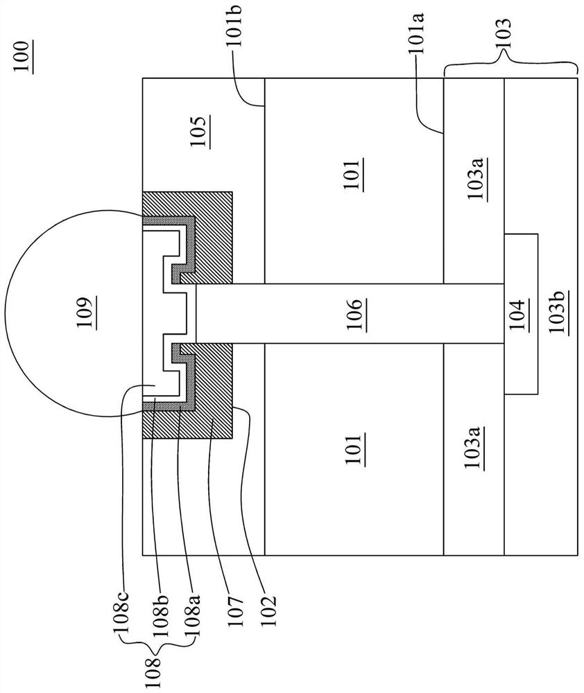
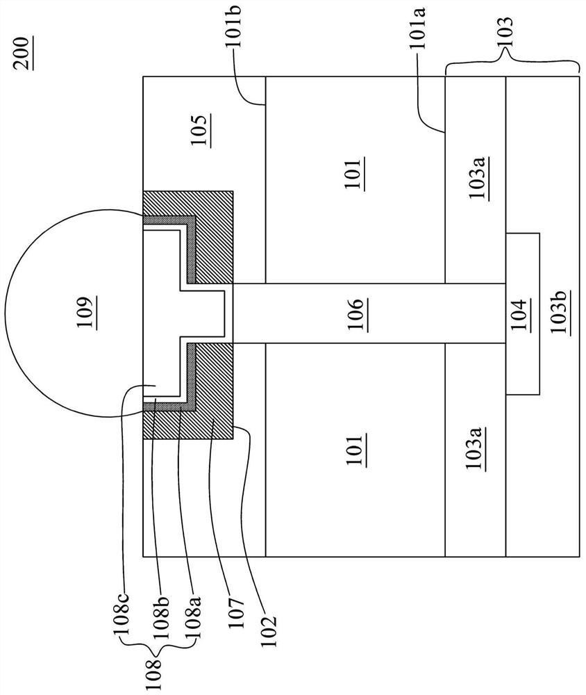
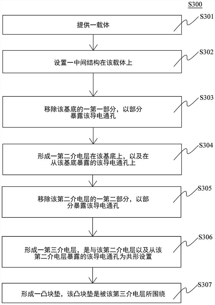
[0072] The following description of the present disclosure is accompanied by the drawings, which are incorporated in and constitute a part of the specification, and illustrate embodiments of the present disclosure, however, the present disclosure is not limited to the embodiments. In addition, the following embodiments can be properly integrated to complete another embodiment.

[0073] It should be understood that although the terms "first", "second", "third" etc. may be used herein to describe various elements, components, regions, layers and / or sections, These elements, components, regions, layers and / or sections should not be limited by these terms. These terms are only used to distinguish one element, component, region, layer or section from another element, component, region, layer or section. Therefore, a "first element", "component", "region", "layer" or "section" discussed below may be referred to as a second means , component, region, layer or section without depart...


PUM


Abstract

The present disclosure provides a semiconductor structure and a method of fabricating the semiconductor structure. The semiconductor structure is provided with an organic dielectric layer arranged under a bonding pad and configured to release stress, a substrate, a first dielectric layer, a second dielectric layer, a conductive through hole, a third dielectric layer and a bonding pad. The substrate is provided with a first surface and a second surface, and the second surface is arranged opposite to the first surface; the first dielectric layer is arranged on the first surface of the substrate; the second dielectric layer is arranged on the second surface of the substrate; the conductive through hole extends through the substrate and partially passes through the first dielectric layer and the second dielectric layer; a third dielectric layer disposed within the second dielectric layer and surrounding a portion of the conductive via; the bonding pad is arranged on the third dielectric layer and the conductive through hole; a dielectric constant of the third dielectric layer is substantially different from a dielectric constant of the second dielectric layer.

Description

technical field [0001] This application claims priority and the benefit of U.S. Formal Application No. 16 / 857,906, filed April 24, 2020, the contents of which are hereby incorporated by reference in their entirety. [0002] The present disclosure relates to a semiconductor structure and a method for preparing the semiconductor structure. In particular, it relates to a semiconductor structure and a method for preparing the semiconductor element, the semiconductor structure has an organic dielectric layer, the organic dielectric layer is arranged under a bonding pad, and is configured to release stress, and the semiconductor structure is prepared The method includes disposing the organic dielectric layer, and forming the bonding pad on the organic dielectric layer. Background technique [0003] Semiconductor components are used in different electronic applications, such as personal computers, mobile phones, digital cameras, or other electronic devices. The manufacture of sem...

Claims


Application Information

Patent Timeline
Patent Type & Authority Applications(China)
IPC IPC(8): H01L23/532H01L21/768
CPCH01L23/53295H01L21/76835H01L23/481H01L24/11H01L24/13H01L21/76898H01L24/05H01L2224/0401H01L2224/02126H01L2224/05547H01L2224/05557H01L2224/05559H01L2224/05018H01L2224/05025H01L2224/13023H01L2224/13025H01L23/3192H01L2224/03452H01L2224/0345H01L2224/03616H01L2224/11334H01L2224/1132H01L2224/03002H01L2224/11002H01L24/03H01L24/02H01L23/293H01L2924/00014H01L21/76804
Inventor 施信益
Owner NAN YA TECH
Why Eureka
Try Eureka