Preparation method of III-group oxide film based on beveled corner substrate and epitaxial wafer thereof

A technology of oxide thin film and chamfered angle, which is applied in semiconductor/solid-state device manufacturing, semiconductor devices, electrical components, etc., can solve the problems of unfavorable mass production, single substrate selection, and affecting device performance, etc., so as to facilitate promotion Use, strong process compatibility, cost reduction effect

Active Publication Date: 2021-10-01
UNIV OF SCI & TECH OF CHINA
View PDF11 Cites 0 Cited by
  • Summary
  • Abstract
  • Description
  • Claims
  • Application Information

AI Technical Summary

Problems solved by technology

[0003] High-quality Ga 2 o 3 Thin films mainly rely on homoepitaxial growth, and the required high-quality single crystal Ga 2 o 3 Substrate, expensive, not conducive to mass production
At the same time, homoepitaxial growth and single substrate selection limit Ga 2 o 3 Application of Thin Films to Fabricate Heterojunction Devices
However, in the existing planar heteroepitaxial substrates, the source gas molecules can freely diffuse on the substrate plane during the growth process, and it is easy to produce Ga substrates with different crystal ...

Method used


Image

  • Preparation method of III-group oxide film based on beveled corner substrate and epitaxial wafer thereof
  • Preparation method of III-group oxide film based on beveled corner substrate and epitaxial wafer thereof
  • Preparation method of III-group oxide film based on beveled corner substrate and epitaxial wafer thereof

Examples


Embodiment Construction

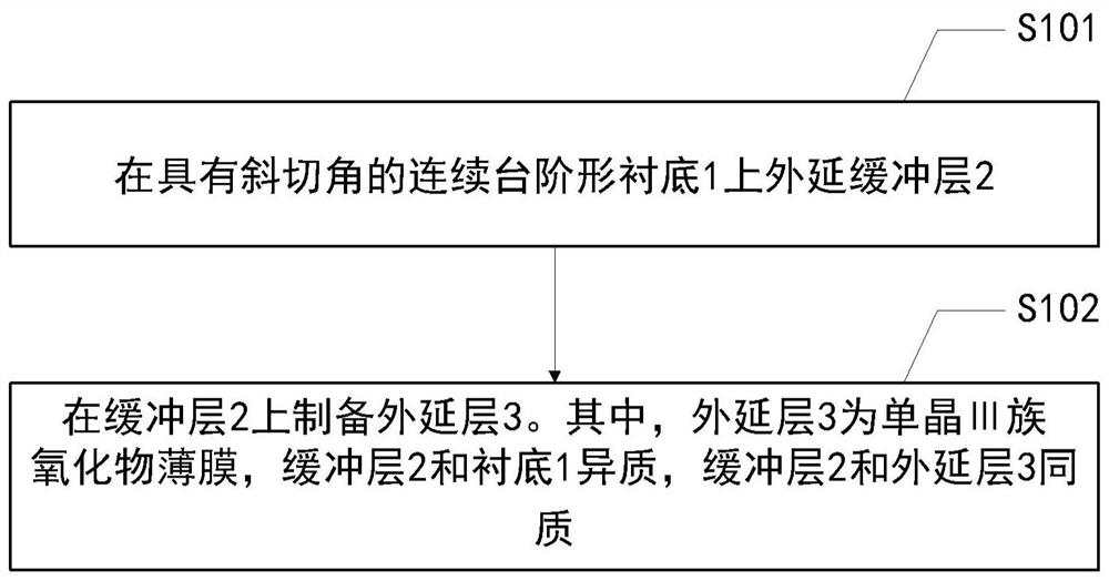
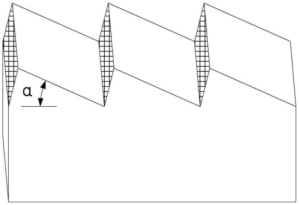
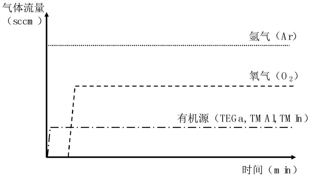
[0034] In order to make the purpose, technical solutions and advantages of the present disclosure clearer, the present disclosure will be further described in detail below in conjunction with specific embodiments and with reference to the accompanying drawings.

[0035] It should be noted that, in the drawings or descriptions of the specification, similar or identical parts all use the same figure numbers. The technical features in the various embodiments exemplified in the specification can be freely combined to form a new solution under the premise of no conflict. In addition, each claim can be used as an embodiment alone or the technical features in each claim can be combined as a new solution. and in the drawings, the shape or thickness of the embodiments may be enlarged, and marked for simplification or convenience. Furthermore, elements or implementations not shown or described in the drawings are forms known to those of ordinary skill in the art. Additionally, while il...


PUM

PropertyMeasurementUnit
Diameteraaaaaaaaaa
Heightaaaaaaaaaa

Abstract

The invention provides a preparation method of a III-group oxide film based on a beveled corner substrate and an epitaxial wafer thereof. The preparation method comprises the following steps of extending a buffer layer (2) on a continuous step-shaped substrate (1) with a beveled corner, preparing an epitaxial layer (3) on the buffer layer (2), wherein the epitaxial layer (3) is a monocrystalline III-group oxide film, the buffer layer (2) and the substrate (1) are heterogeneous, and the buffer layer (2) and the epitaxial layer (3) are homogeneous. By extending the buffer layer on the continuous atomic-scale step-shaped substrate with the beveled corner, adsorption atoms of a reaction source can be promoted to grow at the edge of the step, a consistent-orientation growth mode is formed, a complete monocrystalline buffer layer film is obtained, and then a high-quality monocrystalline epitaxial layer film is formed on the monocrystalline buffer layer film in a homoepitaxial mode. According to the method, the process compatibility is high, the cost for producing the high-quality monocrystalline III-group oxide film is reduced, and the method is convenient to popularize and use.

Description

technical field [0001] The present disclosure relates to the technical field of semiconductors, in particular to a method for preparing a Group III oxide thin film based on an off-cut substrate and an epitaxial wafer thereof. Background technique [0002] Ga 2 o 3 And its homologous oxides are a new generation of ultra-wide bandgap semiconductor materials, which have great application prospects in power electronic devices, microwave devices and deep ultraviolet optoelectronic devices. [0003] High-quality Ga 2 o 3 Thin films mainly rely on homoepitaxial growth, and the required high-quality single crystal Ga 2 o 3 The substrate is expensive and not conducive to mass production. At the same time, homoepitaxial growth and single substrate selection limit Ga 2 o 3 Applications of thin films to fabricate heterojunction devices. However, in the existing planar heteroepitaxial substrates, the source gas molecules can freely diffuse on the substrate plane during the growt...

Claims


Application Information

Patent Timeline
IPC IPC(8): H01L21/02H01L31/0216
CPCH01L21/02554H01L21/02587H01L31/02161
Inventor 孙海定方师汪丹浩梁方舟
Owner UNIV OF SCI & TECH OF CHINA
Why Eureka
Try Eureka