
Device and method for monitoring stripping of protective film for semiconductor substrate

A monitoring device and protective film technology, used in semiconductor/solid-state device manufacturing, measurement devices, optical device exploration, etc., can solve problems such as peeling, and achieve the effect of excellent productivity and commerciality

Pending Publication Date: 2021-09-07
考姆爱斯株式会社
View PDF5 Cites 0 Cited by
  • Summary
  • Abstract
  • Description
  • Claims
  • Application Information

AI Technical Summary

Problems solved by technology

[0006] The purpose of the present invention is to provide a protective film detachment monitoring device for semiconductor substrates that can solve the problem of confirming whether the film is peeled off visually or by non-polarized image analysis, accurately and quickly and automatically judge whether the film is peeled off or whether the film is partially remaining. method

Method used


Image

  • Device and method for monitoring stripping of protective film for semiconductor substrate
  • Device and method for monitoring stripping of protective film for semiconductor substrate
  • Device and method for monitoring stripping of protective film for semiconductor substrate

Examples


Embodiment 1

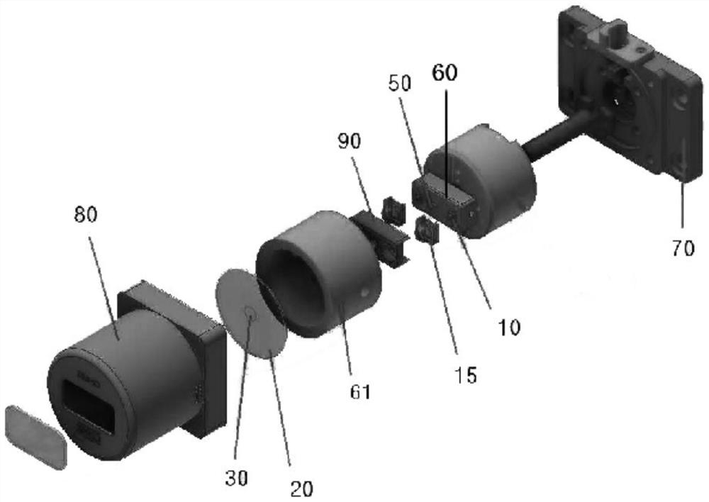
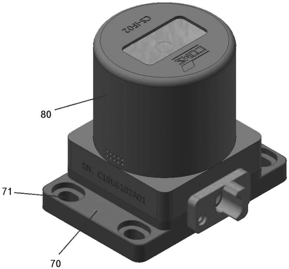
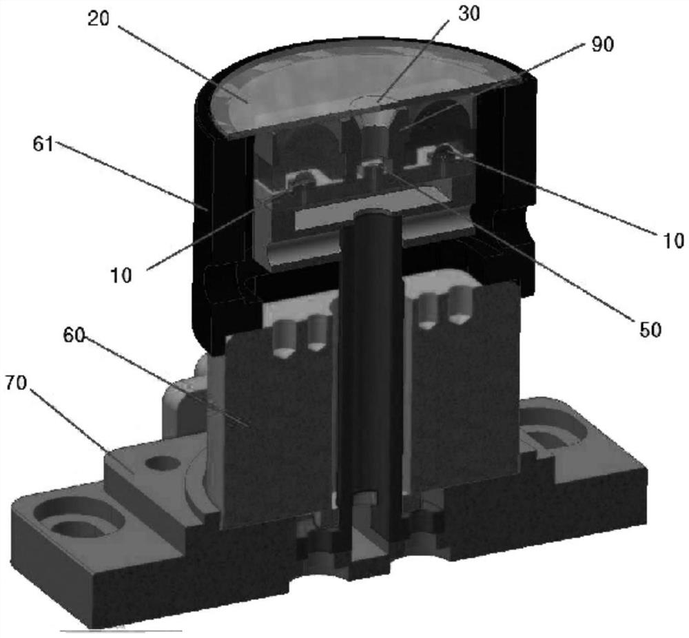
[0046] like Figure 1 to Figure 4 As shown, the semiconductor substrate protective film peeling monitoring device in this embodiment includes a light emitting device 10 , a first polarizer 20 , a second polarizer 30 , a light receiving sensor 50 and a control unit 60 .

[0047] like figure 1 As shown, the first polarizer 20 and the second polarizer 30 can form a circular plate shape, and the second polarizer 30 is located at the center.

[0048] The light-emitting device 10 irradiates light toward the substrate T, that is, the object to be photographed; the first polarizer 20 is located in front of the light-emitting device 10, between the light-emitting device and the substrate, and converts the light generated by the light-emitting device 10 into linearly polarized light, which is directed toward the object to be photographed. incident.

[0049] The second polarizer 30 is perpendicular to the first polarizer 20 , and is located between the substrate T and the light sensor 50...

Embodiment 2

[0075] Figure 9 It is a composition diagram of the monitoring device for whether the protective film for the semiconductor substrate is peeled off in the second embodiment of the present invention;

[0076] Figure 10a and b are diagrams illustrating the polarization cutting effect in Example 2 of the present invention; Figure 10a is the image obtained under non-polarized illumination; Figure 10b It is an image with reflected light removed. The portion removed from the polyester film appears dark due to the removed reflected light, but the portion attached to the polyester film is elliptically polarized, and the light passes through the filter to appear bright.

[0077] Figure 11 It is a partial configuration diagram of a device for monitoring whether or not a protective film for a semiconductor substrate has been peeled in the second embodiment of the present invention.

[0078] like Figure 9 to Figure 11 As shown, whether the semiconductor substrate protective film...


PUM


Abstract

The invention relates to the technical field of PCB production, in particular to a device and method for monitoring whether a protective film for a semiconductor substrate is peeled off or not. The device comprises a light-emitting device which forwards irradiates light towards a substrate, namely a shooting object; a first polarizer which is located in front of the light-emitting device and converts the light generated by the light-emitting device into linearly polarized light, wherein the linearly polarized light is incident in the direction of a subject to be imaged; a second polarizer which has orthogonality with the first polarizer, is positioned between the substrate and a light receiving sensor, and converts the first reflected light reflected by the substrate into second reflected light, wherein the light passes through the direction of the light receiving sensor; a light receiving sensor which receives the light that has passed through the second polarizer, generates a light-dependent electrical signal, and transmits the light-dependent electrical signal to a control unit; and a control unit that determines whether or not a film remains on the surface of the substrate T to be inspected on the basis of the light-related electrical signal or the light intensity value transmitted from the light-receiving sensor.

Description

technical field [0001] The invention relates to the technical field of PCB board production, in particular to a device and method for monitoring whether a protective film for a semiconductor substrate is peeled off. Background technique [0002] Authorized Patent No. 10-1119571 discloses an automatic protective film peeling machine for a semiconductor printed circuit board and a film peeling method. It provides an automatic protective film peeling machine for a semiconductor printed circuit board, which is characterized in that it includes: a loader, and the loader will The substrate with the film attached on the upper and lower sides is loaded on the workbench; the positioner, which positions the substrate on the workbench; the scratcher, which is on the film side (substrate travel direction side) The upper and lower scratches are formed on the edge to form a gap between the substrate and the film; the upper shuttle is configured to absorb the upper part of the substrate on...

Claims


Application Information

Patent Timeline
Patent Type & Authority Applications(China)
IPC IPC(8): G01V8/10
CPCG01V8/10G01N21/958G01N21/8422H01L21/67242H01L21/67132G01N2021/8427G01N2201/0683
Inventor 黄善伍
Owner 考姆爱斯株式会社
Learn More