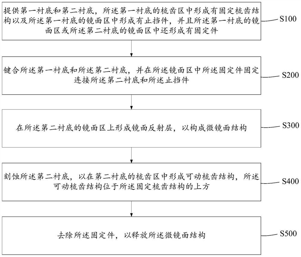
MEMS driving device and forming method thereof
A technology for driving devices and graphics, which is applied to electric solid-state devices, semiconductor devices, and semiconductor/solid-state device components, etc., can solve problems such as etching damage to the sidewalls of comb teeth, and achieve the effect of preventing fracture and improving etching damage.
- Summary
- Abstract
- Description
- Claims
- Application Information
AI Technical Summary
Problems solved by technology
Method used
Image

Examples
Embodiment 1
[0053] Figure 2-Figure 10 It is a schematic diagram of the structure of the method for forming the MEMS driving device in the first embodiment of the present invention during its preparation process.
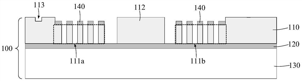
[0054] In step S100, refer to figure 2 and Figure 5 As shown, a first substrate 100 and a second substrate 200 are provided. Wherein, a fixed comb structure is formed in the comb region of the first substrate 100 and a stopper 112 is formed in the mirror region of the first substrate 100, and the stopper 112 corresponds to the The movable part in the mirror area of the second substrate 200 is used to limit the maximum twist angle of the movable part.
[0055] Specifically, both the first substrate 100 and the second substrate 200 have a first comb-tooth area and a second comb-tooth area corresponding to each other, and the mirror area is located between the first comb-tooth area and the second comb-tooth area. Between the second comb tooth area. Correspondingly, the fi...
Embodiment 2
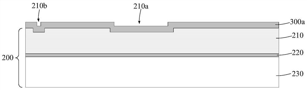
[0105] The difference from Embodiment 1 is that in this embodiment, the fixing member is disposed on the first substrate. The following combination Figure 11 To illustrate, among them, Figure 11It is a structural diagram of the MEMS driving device in the second embodiment of the present invention during its preparation process.
[0106] refer to Figure 11 As shown, the fixing member 300 is directly disposed on the stopper 112 and is located at the edge of the stopper 112 . Wherein, the fixing member 300 may be composed of the first mask layer 140 . And, the first mask layer 140 can also be used to implement the subsequent bonding process, so the first mask layer 140 on the first conductive material layer 110 is retained. Specifically, when bonding the first substrate 100 and the second substrate 200, the first mask layer 140 and the second conductive material layer 210 are bonded to each other (such as silicon-silicon oxide Bond).
[0107] Further, the first mask laye...
Embodiment 3
[0109] The difference from the second embodiment is that the stoppers in this embodiment are only arranged at the edge of the mirror area. The following combination Figure 12 To illustrate, among them, Figure 12 It is a structural schematic diagram of the MEMS driving device in the third embodiment of the present invention during its preparation process.
[0110] refer to Figure 12 As shown, the stopper 112 is only provided at the edge of the mirror area, so that after the micro mirror structure is released, the twist angle of the micro mirror structure can be limited at the edge. Wherein, the stopper 112 is, for example, arranged around the edge of the mirror area, specifically, may be continuously around the edge of the mirror area, or may be discontinuously around the edge of the mirror area.
[0111] In this embodiment, the fixing member 300 may be disposed on the stopper 112 , and the fixing member 300 may be formed by the first mask layer 140 . And, the stopper 11...
PUM
| Property | Measurement | Unit |
|---|---|---|
| Resistance | aaaaa | aaaaa |
Abstract
Description
Claims
Application Information
 - R&D
- Intellectual Property
- Life Sciences
- Materials
- Tech Scout
- Unparalleled Data Quality
- Higher Quality Content
- 60% Fewer Hallucinations
Browse by: Latest US Patents, China's latest patents, Technical Efficacy Thesaurus, Application Domain, Technology Topic, Popular Technical Reports.
© 2025 PatSnap. All rights reserved.Legal|Privacy policy|Modern Slavery Act Transparency Statement|Sitemap|About US| Contact US: help@patsnap.com