
Display device and binding method thereof

Pending Publication Date: 2021-06-25
BOE TECH GRP CO LTD +1
View PDF0 Cites 4 Cited by
  • Summary
  • Abstract
  • Description
  • Claims
  • Application Information

AI Technical Summary

Problems solved by technology

[0003] The distribution mode of the pads of the driving circuit board in the prior art is as follows: figure 1 As shown, the pads at the output end of the driver circuit board are distributed in a straight line, and the abdomen of the driver chip lacks the supporting force. During the bonding process, there is serious collapse and deformation of the abdomen of the driver chip; Uneven indentation leads to poor contact; due to the shrinkage and peeling problems of the anisotropic conductive adhesive film and the glass film, it is easy to cause the conductive particles in the anisotropic conductive adhesive film to fall off and cause misconduction.

Method used


Image

  • Display device and binding method thereof
  • Display device and binding method thereof
  • Display device and binding method thereof

Examples


Embodiment Construction

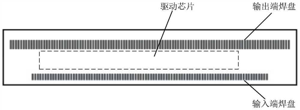
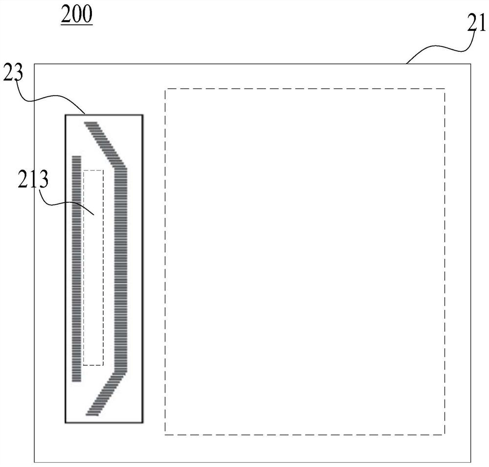
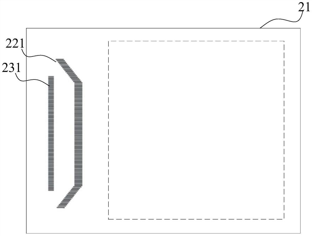
[0041] In order to illustrate the present invention more clearly, the present invention will be further described below in conjunction with preferred embodiments and accompanying drawings. Similar parts in the figures are denoted by the same or similar reference numerals. Those skilled in the art should understand that the content specifically described below is illustrative rather than restrictive, and should not limit the protection scope of the present invention.

[0042] It should be noted that "has", "comprises" and "including" described in the present invention are all open meanings, that is, when the description module "has", "comprises" or "comprises" the first element, the second When referring to a second element and / or a third element, it means that the module includes other elements besides the first element, the second element and / or the third element. In addition, ordinal numerals such as "first", "second" and "third" in the present invention are not intended to...


PUM


Abstract

The invention discloses a display device and a binding method thereof. The display device comprises a display panel and a driving circuit board, the driving circuit board comprises a driving chip, a first bonding pad area and a second bonding pad area, the first bonding pad area and the second bonding pad area are electrically connected with the driving chip and bound with the display panel, the first bonding pad area comprises a plurality of first bonding pads, the first bonding pad area comprises at least one bending part, and the second bonding pad area comprises a plurality of second bonding pads; and the display panel comprises a third bonding pad area bound with the first bonding pad area and a fourth bonding pad area bound with the second bonding pad area, the third bonding pad area comprises a plurality of third bonding pads, the third bonding pads are in one-to-one correspondence with the first bonding pads, the fourth bonding pad area comprises a plurality of fourth bonding pads, and the fourth bonding pads are in one-to-one correspondence with the second bonding pads. According to the display device provided by the invention, the first bonding pad area at least comprising one bending part is arranged, so that collapse of the belly of the chip caused by a binding process in the binding process can be avoided, and the display device has a wide application prospect.

Description

technical field [0001] The present invention relates to the field of display technology, in particular to a display device and a binding method thereof. Background technique [0002] Generally, a display device includes a display panel and a driving circuit board bound thereto. Input terminal pads and output terminal pads connected to the driving chip are arranged on the driving circuit board, and are bound to the display panel through the pads. The area of ​​the transistor array substrate of the display panel is covered with signal lines and thin film transistors, and the fan-out lines of the display panel are connected to the data lines of the array substrate and the pads of the output end of the driving circuit board. [0003] The distribution mode of the pads of the driving circuit board in the prior art is as follows: figure 1 As shown, the pads at the output end of the driver circuit board are distributed in a straight line, and the abdomen of the driver chip lacks th...

Claims


Application Information

Patent Timeline
Patent Type & Authority Applications(China)
IPC IPC(8): G09F9/30
CPCG09F9/30
Inventor 杨心澜王世君冯博刘屹台玉可丁腾飞王洋魏旃樊君吕广爽陈公达张永忠
Owner BOE TECH GRP CO LTD
Learn More