Multilayer transparent conductive anti-reflection film LED chip

A technology of LED chips and anti-reflection films, applied in circuits, electrical components, semiconductor devices, etc., can solve problems such as reduced work efficiency, impact on normal use, and inconvenience to users, and achieve the effect of improving work efficiency and improving service life

Active Publication Date: 2021-06-18
TONGHUI ELECTRONICS
View PDF4 Cites 0 Cited by
  • Summary
  • Abstract
  • Description
  • Claims
  • Application Information

AI Technical Summary

Problems solved by technology

[0003] The current common specifications of LED chips are 38*38mil, 40*40mil, and 45*45m. When in use, the chip will be installed, but because the LED chip is relatively small, the traditional way is to install it through Bolts or superglue fix the chip, but this method is inconvenient to install. Human error or external factors will cause the chip itself to be scratched or damaged, affecting normal use, resulting in a decrease in work efficiency, and giving user inconvenience

Method used


Image

  • Multilayer transparent conductive anti-reflection film LED chip
  • Multilayer transparent conductive anti-reflection film LED chip
  • Multilayer transparent conductive anti-reflection film LED chip

Examples


Embodiment 1

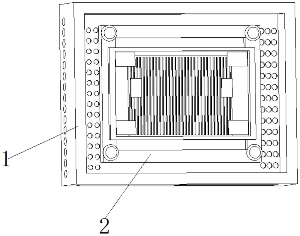
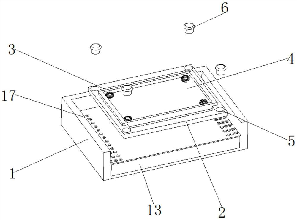
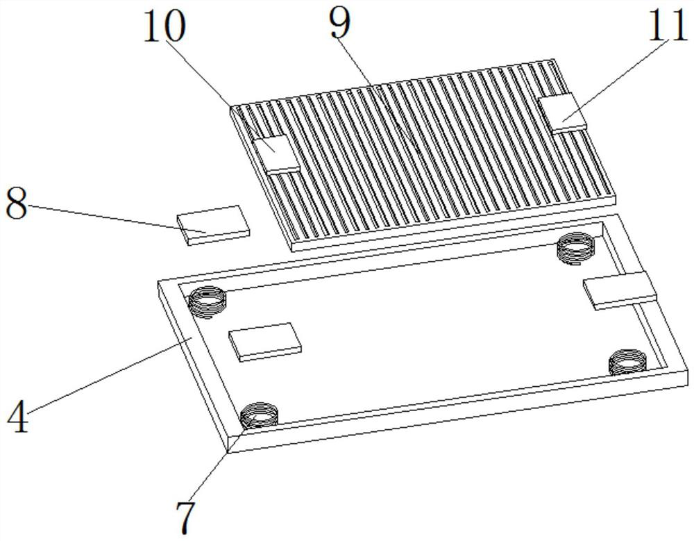
[0030] See Figure 1-5 A multi-layer transparent conductive, an increased film LED chip, including a casing 1, a metal seat 2 in the inside of the casing 1, and a card slot 3 is opened in both sides of the metal seat 2, each card slot. 3 There is a chip base 4, and the compression spring 7 is attached to the inside of the interior bottom surface of the chip base 4, and the upper surface of each of the compression spring 7 is fixedly mounted, and the upper surface of the chip base 4 is mounted. The chip body 9, the central surface of the chip body 9 is fixed to the middle position of the upper surface, and the positive electrode 10 is attached. The central portion of the upper surface of the chip body 9 is fixedly mounted with the negative electrode 11, the chip base 4 and each card slot 3 is attached, the chip base 4 Parallel with the card slot 3, the mounting hole 5 is opened at the surface of the metal seat 2, and each mounting hole 5 is provided with a bolt 6, and the metal seat...

Embodiment 2

[0032] Based on the example one, such as Figure 1-5 Since the outer side of the casing 1 is opened on both sides of the bottom surface of the casing, there is a diaphragm 12 in the lower end of the casing 1, and the mounting chamber 12 is fixed in the middle of the bottom surface of the mounting chamber 12 fixed to the drive motor 14, the drive motor 14 side. The roller 15 is provided, and a plurality of sectors 16 are fixedly mounted on one side surface of the roller 15. The output end of the drive motor 14 is fixed to the roller 15, and each fan blade 16 is not in contact with the surface of the mounting chamber 12. There is a safety cover 13 on the front, and the safety cover 13 is rotated by the mounting chamber 12 by a spring homer, and a plurality of heat dissipating holes 18 are opened at the lower end of the outer surface of the casing 1, each of which extends through the side surface of the casing 1. The mounting chamber 12 is inside, and the mounting chamber 12 is fixedl...


PUM


Abstract

The invention relates to the technical field of LED chips, and discloses a multilayer transparent conductive anti-reflection film LED chip. The chip comprises a box body, a metal base is arranged on the surface of the bottom end in the box body, clamping grooves are formed in the surfaces of the two sides in the metal base, and a chip base is arranged in each clamping groove. Compression springs are fixedly installed at the four corners of the surface of the bottom end in the chip base, and a pressing plate is fixedly installed on the surface of the upper end of each compression spring. According to the multilayer transparent conductive anti-reflection film LED chip, the clamping grooves are formed in the two sides of the interior of the metal base and used for fixing and installing the chip base, each pressing plate is pulled to enable each compression spring to stretch upwards, the chip body is placed in the chip base, then each pressing plate is loosened to enable each compression spring to restore, the chip can be rapidly installed, the phenomenon that the chip is scratched and damaged due to manual operation errors or external factors is avoided, and the working efficiency is effectively improved.

Description

Technical field [0001] The present invention relates to the field of LED chip, in particular a multi-layer transparent conductive, an increased film LED chip. Background technique [0002] The LED chip is a solid-state semiconductor device. The heart of the LED is a semiconductor wafer. At one end of the wafer is attached to a bracket, one end is a negative electrode, and the other end is connected to the positive electrode of the power supply, so that the entire wafer is encapsulated by the epoxy resin, also The LED light-emitting chip is the core component of the LED lamp. Its main function is to convert the electrical energy into light energy, the main material of the chip is single crystal silicon, which has a certain multilayer transparent conductive and diaphragm performance, semiconductor wafer Composed of two parts, part of the P-type semiconductor, dominate in it, the other end is the n-type semiconductor, mainly electrons here, but when these two semiconductors are conn...

Claims


Application Information

Patent Timeline
Patent Type & Authority Applications(China)
IPC IPC(8): H01L23/32H01L23/467H01L23/04H01L33/00
CPCH01L23/32H01L23/467H01L23/04H01L33/00
Inventor 唐景庭田志怀唐兰香皮义群孟立智张江鹏
Owner TONGHUI ELECTRONICS
Why Eureka
Try Eureka