Liquid crystal display substrate, forming method thereof, liquid crystal display panel and forming method of liquid crystal display panel

A liquid crystal display and substrate technology, applied in nonlinear optics, instruments, optics, etc., can solve problems such as poor performance of liquid crystal display substrates, achieve the effects of benefiting accuracy, improving performance, and meeting process requirements

Inactive Publication Date: 2021-06-18
INESA DISPLAY MATERIALS
View PDF5 Cites 0 Cited by
  • Summary
  • Abstract
  • Description
  • Claims
  • Application Information

AI Technical Summary

Problems solved by technology

[0005] However, the existing liquid crystal display substrates formed by COA technology have poor performance

Method used


Image

  • Liquid crystal display substrate, forming method thereof, liquid crystal display panel and forming method of liquid crystal display panel
  • Liquid crystal display substrate, forming method thereof, liquid crystal display panel and forming method of liquid crystal display panel
  • Liquid crystal display substrate, forming method thereof, liquid crystal display panel and forming method of liquid crystal display panel

Examples


Embodiment Construction

[0030] As mentioned in the background art, the performance of existing liquid crystal display substrates is relatively poor.

[0031] The reasons for the poor performance of the liquid crystal display substrate will be described in detail below in conjunction with the accompanying drawings. Figure 1 to Figure 4 It is a structural schematic diagram of each step of a method for forming a liquid crystal display substrate.

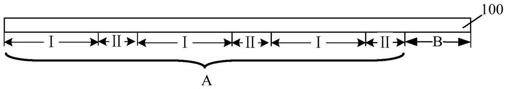
[0032] Please refer to figure 1 , providing a first substrate 100, the first substrate 100 includes: a display area A and a non-display area B, and several transparent areas I and several light-shielding areas II, and the light-shielding areas I are located between adjacent light-transmitting areas II .

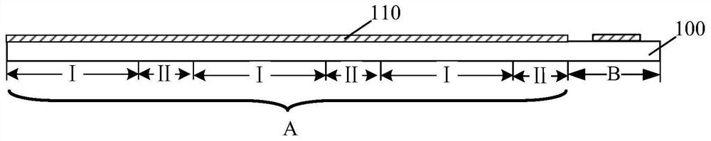
[0033] Please refer to figure 2 , forming a pixel electrode layer 110 on the display area A and part of the non-display area B.

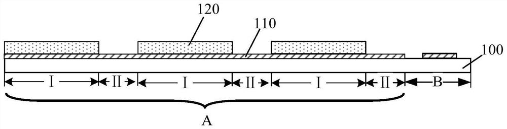
[0034] Please refer to image 3 , forming a color photoresist layer 120 on the light-transmitting region I.

[0035] Plea...


PUM

PropertyMeasurementUnit
wavelengthaaaaaaaaaa

Abstract

The invention discloses a liquid crystal display substrate, a forming method thereof, a liquid crystal display panel and a forming method of the liquid crystal display panel. The forming method of the liquid crystal display substrate comprises the steps that a first substrate is provided, wherein the first substrate comprises a display area and a non-display area, the display area comprises a plurality of transparent areas and a plurality of shading areas, and the shading areas are located between the adjacent transparent areas; a shading material film is formed on the display area and the non-display area, wherein the shading material film has a first optical density; and the shading material film is patterned, and a shading layer is formed on the shading area, wherein the shading layer has second optical density, and the second optical density is larger than the first optical density. According to the method, the alignment accuracy can be improved, and the performance of the formed liquid crystal display substrate and the liquid crystal display panel is good.

Description

technical field [0001] The invention relates to the field of display technology, in particular to a liquid crystal display substrate and a forming method thereof, a liquid crystal display panel and a forming method thereof. Background technique [0002] Liquid crystal display substrate is the most widely used flat-panel display due to its advantages of high display quality, low price, and portability. A monitor with a high-resolution color screen is widely used as a computer screen or a laptop screen. [0003] Most of the liquid crystal display panels currently on the market are backlight liquid crystal display panels, which include a liquid crystal display substrate and a backlight module. Usually, the liquid crystal display substrate is composed of a color filter substrate (Color Filter, CF), a thin film transistor array substrate (Thin Film Transistor Array Substrate, TFT Array Substrate), and a liquid crystal layer (Liquid Crystal Layer) arranged between the two substra...

Claims


Application Information

Patent Timeline
Patent Type & Authority Applications(China)
IPC IPC(8): G02F1/1335
CPCG02F1/133512G02F1/133514
Inventor 李欣范刚洪陈黛黛王红光张莉
Owner INESA DISPLAY MATERIALS
Why Eureka
Try Eureka