Resonator and method for manufacturing resonator
A manufacturing method and resonator technology, applied in impedance networks, electrical components, etc., can solve the problem that SAW resonators cannot meet the requirements of large-bandwidth communication, and achieve the effect of no stray FOM and large bandwidth
- Summary
- Abstract
- Description
- Claims
- Application Information
AI Technical Summary
Problems solved by technology
Method used
Image
Examples
Embodiment 1
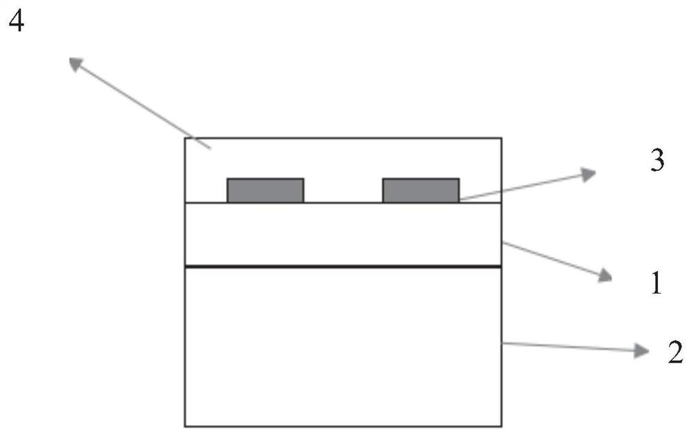
[0049] Below, refer to Figure 1 to Figure 12 The resonator according to the present invention will be described.
[0050] First, use figure 1 The structure of the resonator according to the present invention will be described.
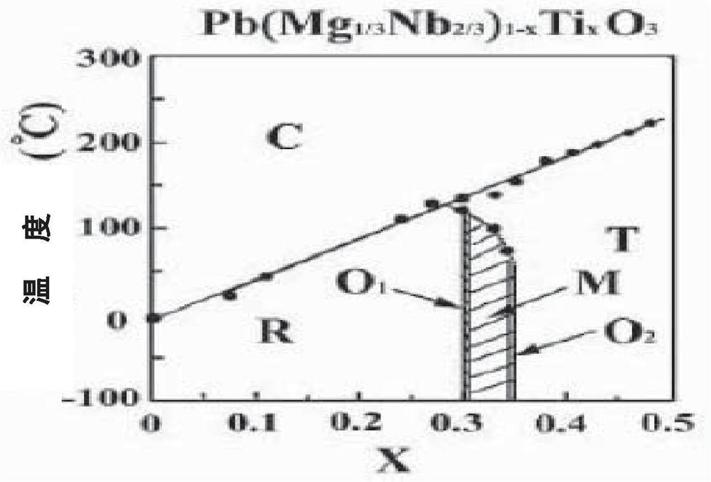
[0051] figure 1 is a schematic diagram of a resonator involved in the present invention. In the resonator of this embodiment, the material of the substrate 2 may be a high-sonic layer material, preferably SiC, SiN, diamond, Si and the like. The thickness of the substrate 2 can be adjusted according to product design, preferably 350 μm˜500 μm. A piezoelectric layer 1 is formed on a substrate 2 . The thickness of the piezoelectric layer 1 can be determined according to the wavelength λ of the acoustic wave excited by the electrode fingers (as an example, λ=1 μm), for example, it can be 0.1λ˜2λ. In this embodiment, the material of piezoelectric layer 1 is PMNT single crystal, its chemical formula (1-x)Pb(Mg 1 / 3 Nb 2 / 3 )O 3 -xPbTiO 3 where x=0...
Embodiment 2
[0072] Below, refer to Figure 13 as well as Figure 14 A method for manufacturing the resonator according to the present invention will be described in detail.
[0073] Figure 13 is a schematic diagram of the manufacturing method of the resonator according to the present embodiment, and Figure 14 is a flowchart of the manufacturing method of the resonator according to the present embodiment.
[0074] The manufacturing method of the resonator in this embodiment starts with step S1401. In this step S1401, as Figure 13 As shown in a, a substrate 22 may be provided. The material of the substrate 22 may be a high-sonic layer material, preferably SiC, SiN, diamond, Si and the like. The thickness of the substrate 22 can be adjusted according to product design, preferably 350 μm˜500 μm.
[0075] Next, in step S1402, the piezoelectric layer 21 can be combined with the substrate 22 through low-temperature bonding, such as Figure 13 Shown in b. As an example, the low temper...
PUM
| Property | Measurement | Unit |
|---|---|---|
| thickness | aaaaa | aaaaa |
| thickness | aaaaa | aaaaa |
| frequency | aaaaa | aaaaa |
Abstract
Description
Claims
Application Information
 - R&D
- Intellectual Property
- Life Sciences
- Materials
- Tech Scout
- Unparalleled Data Quality
- Higher Quality Content
- 60% Fewer Hallucinations
Browse by: Latest US Patents, China's latest patents, Technical Efficacy Thesaurus, Application Domain, Technology Topic, Popular Technical Reports.
© 2025 PatSnap. All rights reserved.Legal|Privacy policy|Modern Slavery Act Transparency Statement|Sitemap|About US| Contact US: help@patsnap.com


