Power device module and manufacturing method thereof

A technology for power devices and manufacturing methods, which is applied in semiconductor/solid-state device manufacturing, semiconductor devices, electric solid-state devices, etc., can solve the problems of large-scale application of unfavorable devices and high manufacturing costs

Active Publication Date: 2021-06-08
INST OF MICROELECTRONICS CHINESE ACAD OF SCI
View PDF8 Cites 0 Cited by
  • Summary
  • Abstract
  • Description
  • Claims
  • Application Information

AI Technical Summary

Problems solved by technology

However, the manufacturing cost of existing GaN-based power devices is still high, which is not conducive to the large-scale application of devices

Method used


Image

  • Power device module and manufacturing method thereof
  • Power device module and manufacturing method thereof
  • Power device module and manufacturing method thereof

Examples


Embodiment Construction

[0043] The above is the core idea of ​​the present invention. In order to make the above-mentioned purposes, features and advantages of the present invention more obvious and easy to understand, the technical solutions in the embodiments of the present invention will be clearly and completely described below in conjunction with the accompanying drawings in the embodiments of the present invention Description, obviously, the described embodiments are only a part of the embodiments of the present invention, rather than all the embodiments. Based on the embodiments of the present invention, all other embodiments obtained by persons of ordinary skill in the art without making creative efforts belong to the protection scope of the present invention.

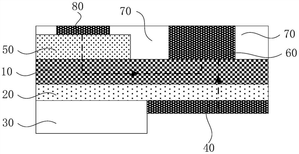
[0044] An embodiment of the present invention provides a power device module, such as figure 1 shown, including:

[0045] a first doped semiconductor layer 10;

[0046] The second doped semiconductor layer 20 located on one side sur...


PUM

PropertyMeasurementUnit
thicknessaaaaaaaaaa
thicknessaaaaaaaaaa
thicknessaaaaaaaaaa

Abstract

The invention provides a power device module and a manufacturing method thereof. The power device module comprises a first semiconductor doping layer; a second semiconductor doping layer positioned on one side of the first semiconductor doping layer; a substrate and a first anode located on the surface of the side, away from the first semiconductor doping layer, of the second semiconductor doping layer; a third semiconductor doping layer, a cathode and an insulating medium layer located on the other side of the first semiconductor doping layer; and a second anode positioned on the surface of the third semiconductor doped layer; wherein the first anode, the third semiconductor doping layer, the first semiconductor doping layer and the cathode form a first diode, the second anode, the second semiconductor doping layer, the first semiconductor doping layer and the cathode form a second diode, and the first diode and the second diode are connected in parallel, so that under the condition that the area of the wafer is not expanded, by manufacturing the second diode on the other side of the substrate, the cascade connection of the two diodes is realized, the integration level of the power device module is improved, and the cost of the power device module is reduced.

Description

technical field [0001] The invention relates to the technical field of semiconductors, and more specifically, to a power device module and a manufacturing method thereof. Background technique [0002] As a third-generation semiconductor material, gallium nitride (GaN) has the advantages of large band gap, high drift velocity of saturated electrons, strong critical breakdown electric field, and high thermal conductivity. It is used in extreme working environments such as high voltage, high frequency, and high power. It has huge application potential, therefore, it has obvious potential advantages in the production of high-performance power semiconductor devices, especially in the production of power electronic devices with high speed, low power consumption, and medium and low voltage operations. However, the manufacturing cost of the existing GaN-based power devices is still high, which is not conducive to the large-scale application of the devices. Contents of the inventio...

Claims


Application Information

Patent Timeline
Patent Type & Authority Applications(China)
IPC IPC(8): H01L27/08H01L21/8252
CPCH01L27/0814H01L21/8252
Inventor 赵媛媛郑英奎康玄武孙跃
Owner INST OF MICROELECTRONICS CHINESE ACAD OF SCI
Why Eureka
Try Eureka