Multi-chip mounting structure and manufacturing method thereof

A multi-chip, mounting technology, applied in semiconductor/solid-state device manufacturing, electrical components, circuits, etc., can solve problems such as difficulty in effectively realizing on-demand filling, difficulty in filling packaging structures, and large influence between steps, etc. Improve process efficiency and product yield, reduce filling difficulty, and solve the effect of filling bubbles

Active Publication Date: 2021-06-22
浙江集迈科微电子有限公司
View PDF3 Cites 0 Cited by
  • Summary
  • Abstract
  • Description
  • Claims
  • Application Information

AI Technical Summary

Problems solved by technology

[0005] In view of the above-mentioned shortcomings of the prior art, the object of the present invention is to provide a chip mount structure and a method for preparing the chip mount structure, which are used to solve the problem of the difficulty in forming an effective underfill at the bottom of a multi-chip structure in the prior art. The packaging structure of the chip integration is difficult to fill, the process is complicated, the influence between steps is large, and it is difficult to effectively realize on-demand filling.

Method used


Image

  • Multi-chip mounting structure and manufacturing method thereof
  • Multi-chip mounting structure and manufacturing method thereof
  • Multi-chip mounting structure and manufacturing method thereof

Examples


Embodiment 1

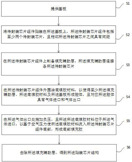
[0038] Such as figure 1 As shown, the present invention provides a kind of preparation method of multi-chip mounting structure, and described preparation method comprises the following steps:

[0039] S1, providing the substrate;

[0040] S2, attaching a chip assembly to be packaged on the substrate, the chip assembly to be packaged includes at least two chips to be packaged, and there is a distance between adjacent chips to be packaged;

[0041] S3, preparing an auxiliary filling layer on the chip assembly to be packaged, the auxiliary filling layer connecting each of the chips to be packaged;

[0042] S4, coating an underfill material on the periphery of the chip component to be packaged, so that at least the filling auxiliary layer, the underfill material, and the substrate form a cavity, and corresponding to the cavity, there is a gas inlet and a gas exit;

[0043] S5, applying negative pressure at the gas outlet, and correspondingly coating the underfill material at th...


PUM


Abstract

The invention provides a multi-chip mounting structure and a preparation method. The preparation includes: mounting a plurality of chips on a substrate, preparing a filling auxiliary layer on the chip to form a cavity, corresponding to the cavity having a gas inlet and a gas outlet, Apply underfill material at the gas inlet, apply negative pressure at the gas outlet, and based on the air pressure, the underfill material flows into the bottom of the chip to form an underfill. For the packaging structure of multiple chip modules, the present invention builds a cavity between the chip to be packaged and the substrate, applies an underfill material at the gas inlet, and applies negative pressure at the gas outlet, so that the underfill is compressed under the action of air pressure. Inserting into the bottom of the chip can reduce the difficulty of filling the underfill of the multi-chip structure, and is conducive to solving the problem of filling air bubbles. It can also solve the problems of difficult placement of the glue filling head, complicated glue filling process and great influence on the structure of the previous steps in the structure of multi-chip small pitch. The invention has simple process and can also solve the problem of filling on demand when multiple chips are difficult to integrate.

Description

technical field [0001] The invention belongs to the technical field of semiconductors, and in particular relates to a mounting chip structure and a preparation method for the mounting chip structure. Background technique [0002] The bottom mounting technology of the chip is the main way for the chip to be connected to the terminal. In order to prevent the large stress difference between the chip and the substrate from causing the solder balls to break, it is often necessary to fill the bottom glue between the chip and the substrate. [0003] However, with the development of technology, the number of chips has increased and the size has become larger, and the number of chips mounted on the surface of the current module is large. At present, in the prior art, it is difficult to perform bottom filling according to actually needed chips among multiple chips, and not to fill unnecessary chips. In addition, it is very difficult for the underfill to completely occupy the space at...

Claims


Application Information

Patent Timeline
Patent Type & Authority Patents(China)
IPC IPC(8): H01L21/67H01L21/56
CPCH01L21/561H01L21/67121H01L21/67126
Inventor 冯光建顾毛毛黄雷郭西高群
Owner 浙江集迈科微电子有限公司
Why Eureka
Try Eureka