Organic light-emitting device and method of manufacturing organic light-emitting device

A technology of organic light-emitting devices and organic layers, which is applied in the direction of organic semiconductor devices, semiconductor/solid-state device manufacturing, and electric solid-state devices. It can solve problems such as poor electrical conductivity, improve external quantum efficiency, and achieve normal luminous effects.

Active Publication Date: 2021-04-02
KUNSHAN NEW FLAT PANEL DISPLAY TECH CENT
View PDF4 Cites 0 Cited by
  • Summary
  • Abstract
  • Description
  • Claims
  • Application Information

AI Technical Summary

Problems solved by technology

[0003] In view of this, the present invention provides an organic light-emitting device and a method for manufacturing the organic light-emitting device. On the basis of adding a transparent organic layer to the organic light-emitting device, a conductive layer is further added, and the conductive layer is overlapped with the reflective cathode layer, so that First, when a voltage is applied to the organic light-emitting device, the electrons generated by the reflective cathode layer can be injected into the light-emitting layer through the conductive layer, which improves the problem of applying a higher voltage due to the poor conductivity of the transparent organic layer.

Method used


Image

  • Organic light-emitting device and method of manufacturing organic light-emitting device
  • Organic light-emitting device and method of manufacturing organic light-emitting device
  • Organic light-emitting device and method of manufacturing organic light-emitting device

Examples


Embodiment Construction

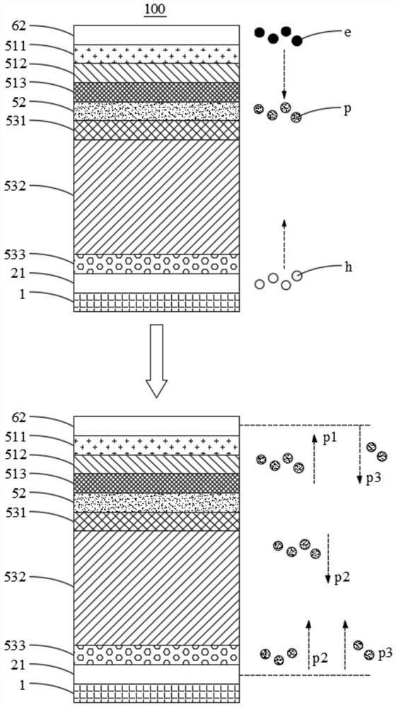
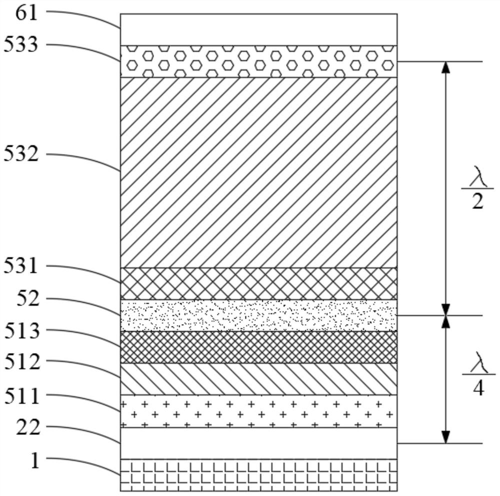
[0033] In order to make the object, technical solution and advantages of the present invention clearer, the present invention will be further described in detail below in conjunction with the accompanying drawings and embodiments. It should be understood that the specific embodiments described here are only used to explain the present invention, not to limit the present invention.

[0034] In describing the present invention, it is to be understood that the terms "central", "lateral", "upper", "lower", "left", "right", "vertical", "horizontal", "top", The orientation or positional relationship indicated by "bottom", "inner" and "outer" is based on the orientation or positional relationship shown in the drawings, and is only for the convenience of describing the present invention and simplifying the description, rather than indicating or implying the referred device Or elements must have a certain orientation, be constructed and operate in a certain orientation, and thus should...


PUM

PropertyMeasurementUnit
Angleaaaaaaaaaa
Thicknessaaaaaaaaaa
Thicknessaaaaaaaaaa

Abstract

The embodiment of the invention provides an organic light-emitting device and a method of manufacturing the organic light-emitting device, after the hierarchical structure of the organic light-emitting device is inverted, a transparent organic layer and a conductive layer are further added, and the conductive layer and a reflective cathode layer are in lap joint. By additionally arranging the transparent organic layer, the micro-cavity structure of the organic light-emitting device can be ensured not to be changed basically after being inverted compared with the micro-cavity structure before being inverted, so that photons generated by the light-emitting layer can be emitted out of the organic light-emitting device, and the external quantum efficiency of the inverted organic light-emittingdevice is improved. By additionally arranging the conductive layer, electrons generated by the reflective cathode layer can be injected into the light-emitting layer through the conductive layer, anda problem that the higher voltage needs to be applied due to poor conductivity of the transparent organic layer is solved. Due to the design, normal luminescence of the organic light-emitting deviceunder normal voltage can be realized on the premise of ensuring that the external quantum efficiency of the inverted organic light-emitting device is not reduced basically.

Description

technical field [0001] The invention belongs to the field of display technology, and in particular relates to an organic light-emitting device and a method for manufacturing the organic light-emitting device. Background technique [0002] In a manufacturing process of an OLED (Organic Light-Emitting Diode, organic light-emitting device) display panel, in order to match a thin film transistor (Thin Film Transistor, TFT) with higher mobility, it is necessary to perform an inverted design on the OLED device to form an inverted OLED device. However, when using an inverted OLED device, generally a higher voltage needs to be applied to ensure that the inverted OLED device can emit light normally. Contents of the invention [0003] In view of this, the present invention provides an organic light-emitting device and a method for manufacturing the organic light-emitting device. On the basis of adding a transparent organic layer to the organic light-emitting device, a conductive lay...

Claims


Application Information

Patent Timeline
IPC IPC(8): H01L51/52H01L51/50H01L51/56H01L27/32
CPCH10K59/00H10K50/80H10K50/82H10K50/824H10K50/85H10K2102/321H10K71/00
Inventor 颜志敏刘俊伟李灏
Owner KUNSHAN NEW FLAT PANEL DISPLAY TECH CENT
Why Eureka
Try Eureka