
IPD absorption band-pass filter

A band-pass filter and absorbing technology, applied in the field of filters, can solve problems such as impedance mismatch, limited filter bandwidth, large space requirements, etc., and achieve high yield and good batch consistency

Pending Publication Date: 2021-02-26
云南雷迅科技有限公司
View PDF0 Cites 2 Cited by
  • Summary
  • Abstract
  • Description
  • Claims
  • Application Information

AI Technical Summary

Problems solved by technology

For example, a low-pass prototype filter and its complementary high-pass filter are connected in parallel to form a complementary duplexer to absorb the stopband signal, but this will require a large space and cause impedance mismatch
Adding two traditional microstrip comb-line bandpass filters between two microstrip 3dB directional couplers can also absorb stopband signals, but the width of the bridge limits the bandwidth of the filter
Connect two equal-phase power dividers at the input and output terminals, and then connect +45 degree high-pass phase shifter, traditional band-pass filter, -45 degree in series to the upper and lower paths between the two power dividers. A low-pass phase shifter, which realizes the phase cancellation function of the input signal and the reflected signal at the input end, although it achieves the effect of absorbing the reflected signal, but requires a large number of circuit components, so for the current miniaturization needs, the lumped circuit It is hindered by the layout and component interaction of the

Method used


Image

  • IPD absorption band-pass filter
  • IPD absorption band-pass filter
  • IPD absorption band-pass filter

Examples


Embodiment Construction

[0024] The present invention will be further described below in conjunction with accompanying drawing.

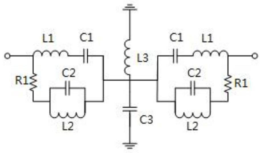
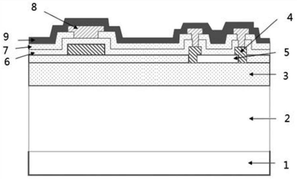
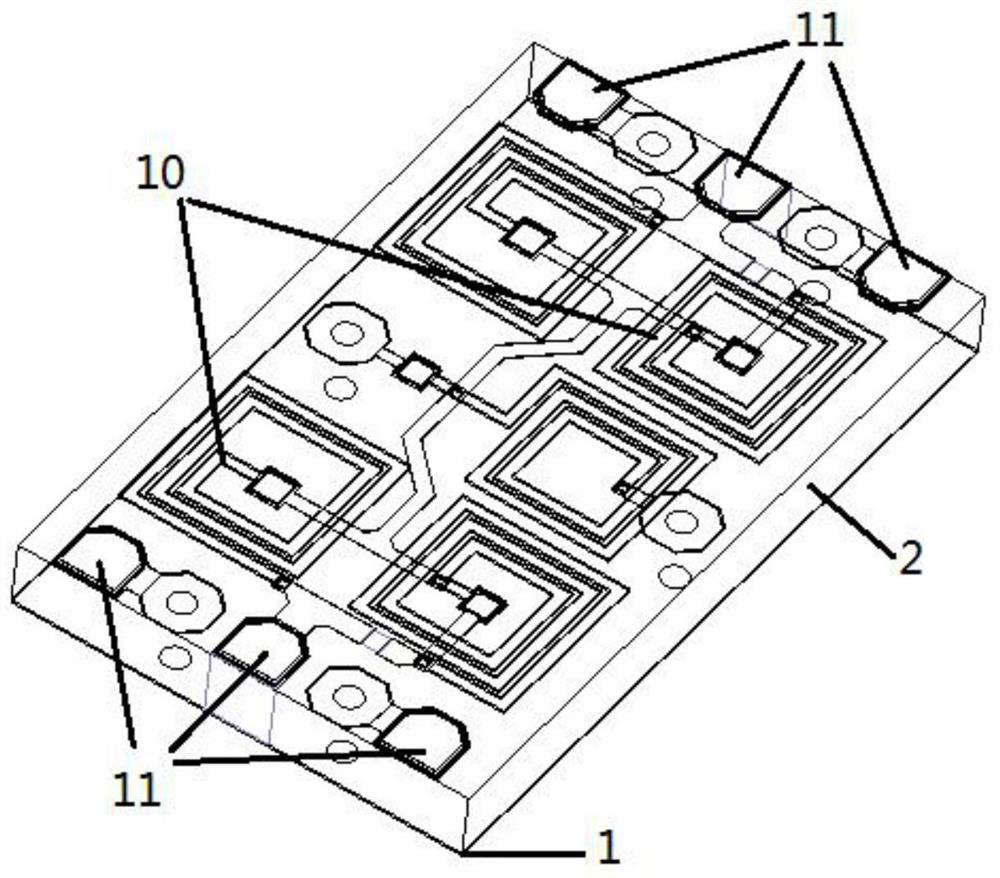
[0025] Such as figure 1 As shown, the absorption bandpass filter of the present invention includes a base layer 2 and a back gold layer 1 on the lower surface of the base layer 2, and also includes a metal layer, which forms a filter circuit structure 10, and the filter circuit structure 10 includes a series The first band-pass signal processing unit and the second-type band-pass signal processing unit between the input port and the output port are provided with a ground port connection between the first band-pass signal processing unit and the second-type band-pass signal processing unit. The basic main circuit of the band-pass filter, the band-pass signal processing unit is composed of the band-pass signal path and the out-of-band absorption branch; the basic main circuit of the band-pass filter is the parallel resonance of the inductance and the capacitor (L3, C3); The ...


PUM

PropertyMeasurementUnit
thicknessaaaaaaaaaa
thicknessaaaaaaaaaa
thicknessaaaaaaaaaa

Abstract

The invention relates to an IPD absorption band-pass filter and belongs to the technical field of filters. The sensor comprises a substrate layer and a back gold layer on the lower surface of the substrate layer, wherein a first silicon nitride layer grows on the substrate layer, a thin-film resistance layer is sputtered on the first silicon nitride layer, a first metal layer is formed on the first silicon nitride layer, a second silicon nitride layer grows on the first metal layer, and a polyimide layer grows on the second silicon chloride layer; a second metal layer is formed on the polyimide layer, a third silicon nitride layer grows on the second metal layer, and a filter circuit structure is formed on the first metal layer and the second metal layer; the filter circuit structure comprises a first band-pass signal processing unit, a second band-pass signal processing unit and an LC parallel resonance circuit which are connected in series between an input port and an output port, anIPD-GaAs process is adopted, the absorption type filter circuit structure is manufactured on a GaAs substrate through photoetching, sputtering, electroplating, etching and other procedures, and the effect of high stop band suppression is achieved.

Description

technical field [0001] The invention relates to an IPD absorption bandpass filter, which belongs to the technical field of filters. Background technique [0002] With the rapid development of communication technology, communication systems have higher and higher requirements for high-performance and miniaturized passive components. Band-pass filters are one of the important electronic components of communication devices, and the performance of band-pass filters directly affects communication systems. performance. Stopband "attenuation" signals in conventional bandpass filters are reflected back to the signal source, however, these reflections can adversely affect the overall RF system. For example, mixers are extremely sensitive to out-of-band terminations on their ports, yet filters are frequently present at the front and back ends of mixers. Intermodulation products attenuated by the filter are reflected back to the mixer and may generate unwanted harmonics that can caus...

Claims


Application Information

Patent Timeline
Patent Type & Authority Applications(China)
IPC IPC(8): H01P1/212H01P1/203H01P11/00
CPCH01P1/203H01P1/212H01P11/007
Inventor 代传相李小珍邢孟江张志刚侯明刘永红
Owner 云南雷迅科技有限公司
Learn More