Chip io pin verification system and method
A verification system and verification method technology, applied in the field of chip IO pin verification system, can solve the problem of low verification coverage of chip IO pins, and achieve the effect of improving efficiency
- Summary
- Abstract
- Description
- Claims
- Application Information
AI Technical Summary
Problems solved by technology
Method used
Image

Examples
Embodiment 1
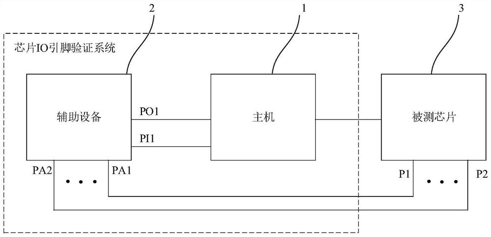
[0044] This embodiment provides a chip IO pin verification system. refer to figure 1 , the chip IO pin verification system includes a host 1 and an auxiliary device 2 . The host 1 is connected to the chip under test 3 and the auxiliary device 2 in communication respectively. The host 1 configures the chip under test 3 to output a preset level signal on the configuration pin according to the preset test configuration; the configuration pin is the pin of the chip under test 3 other than the current pin to be tested, and the configuration pin is the same as the current pin to be tested. The test pins have a preset pairing relationship. In an optional embodiment, the host 1 is implemented by a PC (personal computer).
[0045] The auxiliary device 2 includes a number of auxiliary pins, the number of auxiliary pins is the same as that of the IO pins of the tested chip 3, and each auxiliary pin is electrically connected to an IO pin correspondingly. like figure 1 As shown, the f...
Embodiment 2
[0073] This embodiment provides a chip IO pin verification method. The chip IO pin verification method can be implemented by using the chip IO pin verification system of the first embodiment.
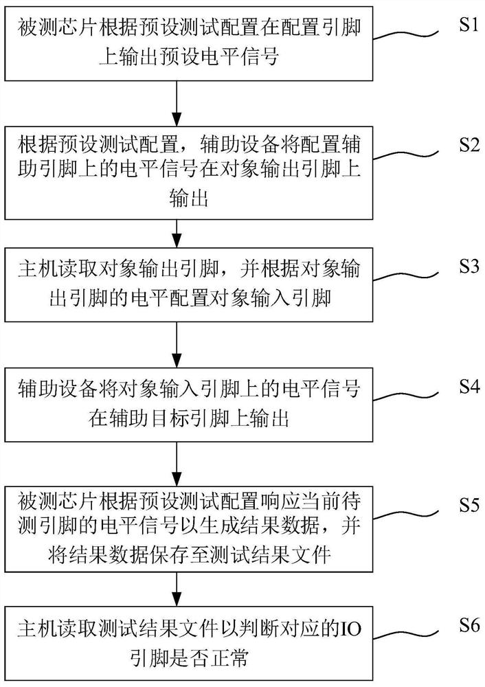
[0074] refer to image 3 , the chip IO pin verification method includes the following steps:
[0075] Step S1, the chip under test outputs a preset level signal on the configuration pin according to the preset test configuration. The configuration pins are pins of the chip under test other than the current pins to be tested, and the configuration pins and the current pins to be tested have a preset pairing relationship.
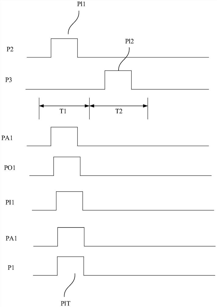
[0076] Step S2, according to the preset test configuration, the auxiliary device outputs the level signal on the configuration auxiliary pin on the object output pin PO1.
[0077] Step S3, the host reads the object output pin PO1, and configures the object input pin PI1 according to the level of the object output pin PO1.
[0078] Step S4, the auxiliary device outp...
PUM
 Abstract
Description
Claims
Application Information
 - R&D
- Intellectual Property
- Life Sciences
- Materials
- Tech Scout
- Unparalleled Data Quality
- Higher Quality Content
- 60% Fewer Hallucinations
Browse by: Latest US Patents, China's latest patents, Technical Efficacy Thesaurus, Application Domain, Technology Topic, Popular Technical Reports.
© 2025 PatSnap. All rights reserved.Legal|Privacy policy|Modern Slavery Act Transparency Statement|Sitemap|About US| Contact US: help@patsnap.com