Display panel, manufacturing method thereof and display device
A display panel and substrate technology, applied in the direction of diodes, semiconductor devices, electrical components, etc., can solve problems such as peeling of the flat layer, poor flattening effect of the flat layer, and affecting product reliability, etc., to achieve good effect, uniform thickness, and reduce flatness The effect of the risk of layer peeling
- Summary
- Abstract
- Description
- Claims
- Application Information
AI Technical Summary
Problems solved by technology
Method used
Image

Examples
Embodiment 1
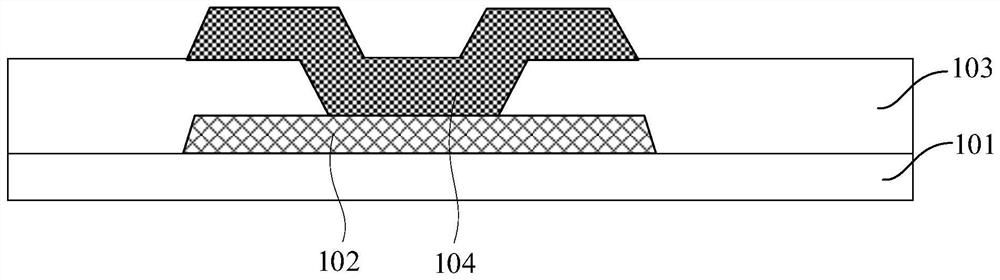
[0041]Referencefigure 2 , Shows a schematic structural diagram of a display panel located in a pixel interval area according to an embodiment of the present invention.
[0042]An embodiment of the present invention provides a display panel, including: a substrate 201, the substrate 201 is divided into a plurality of sub-pixel areas and a pixel interval area located between two adjacent columns of sub-pixel areas; a substrate arranged in the pixel interval area Resistance-reducing wiring 202 on 201; interlayer dielectric layer 203 provided on substrate 201, interlayer dielectric layer 203 has openings exposing resistance-reducing wiring 202; signal lines 204 and signal lines 204 provided in the openings It is connected to the resistance-reducing wiring 202, and the signal line 204 is distributed along the column direction of the display panel, and the width of the opening is greater than or equal to the width of the signal line 204 along the row direction of the display panel.
[0043]Spec...
Embodiment 2
[0082]ReferenceFigure 5, Shows a flowchart of a method for manufacturing a display panel according to an embodiment of the present invention, which may specifically include the following steps:
[0083]In step 501, a substrate is provided; the substrate is divided into a plurality of sub-pixel regions and a pixel interval region located between two adjacent columns of the sub-pixel regions.
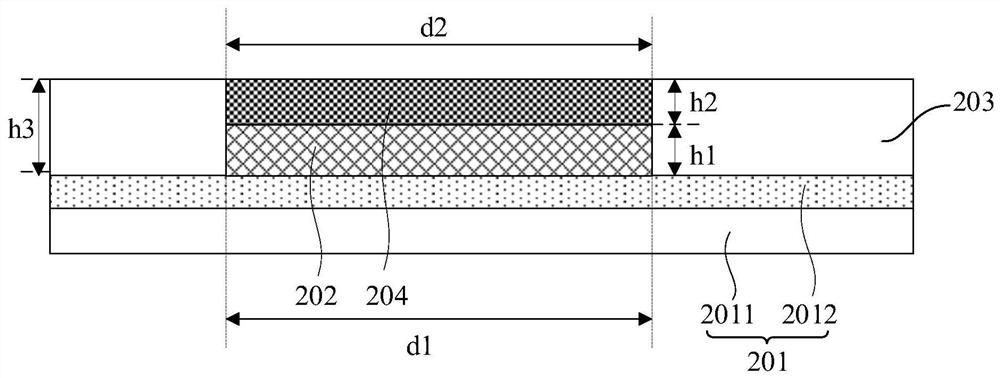
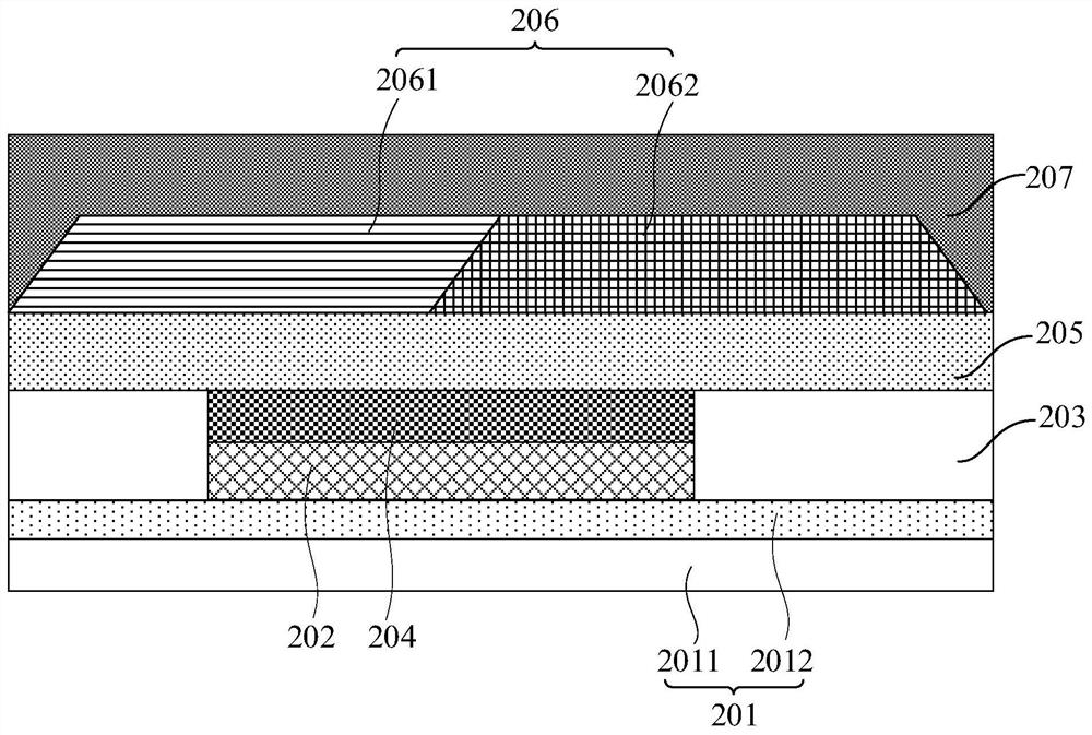
[0084]In the embodiment of the present invention, first, a substrate 201 is provided, and the substrate is divided into a plurality of sub-pixel regions and a pixel interval region located between two adjacent columns of sub-pixel regions.
[0085]The substrate 201 located in the pixel spacing area includes a substrate 2011 and a buffer layer 2012 provided on the substrate 2011; the substrate 201 located in the sub-pixel area includes a substrate 2011, a light shielding layer 2013 provided on the substrate 2011, and a covering light shielding layer 2013 and The buffer layer 2012 of the substrate 2011.
[0...
Embodiment 3
[0105]An embodiment of the present invention provides a display device including the above-mentioned display panel.
[0106]For the specific description of the display panel, reference may be made to the description of Embodiment 1 and Embodiment 2, which will not be repeated in this embodiment of the present invention.
[0107]Of course, the display device also includes a touch panel and the like arranged on the light-emitting surface of the display panel. In addition, the display device also includes a driver chip and a TCON (Timer Control Register, timing controller) device.
[0108]In practical applications, the display device can be any product or component with a display function, such as a mobile phone, a tablet computer, a monitor, a notebook computer, and a navigator.
[0109]In the embodiment of the present invention, the signal line is formed in the opening of the interlayer dielectric layer, and the width of the opening is greater than or equal to the width of the signal line, that ...
PUM
 Abstract
Description
Claims
Application Information
 - R&D
- Intellectual Property
- Life Sciences
- Materials
- Tech Scout
- Unparalleled Data Quality
- Higher Quality Content
- 60% Fewer Hallucinations
Browse by: Latest US Patents, China's latest patents, Technical Efficacy Thesaurus, Application Domain, Technology Topic, Popular Technical Reports.
© 2025 PatSnap. All rights reserved.Legal|Privacy policy|Modern Slavery Act Transparency Statement|Sitemap|About US| Contact US: help@patsnap.com