Pixel structure and preparation method thereof
A pixel structure and pixel technology, applied in semiconductor/solid-state device manufacturing, semiconductor devices, electrical components, etc., can solve the problems of short lifespan and low light extraction efficiency of organic materials
- Summary
- Abstract
- Description
- Claims
- Application Information
AI Technical Summary
Problems solved by technology
Method used
Image
Examples
Embodiment Construction
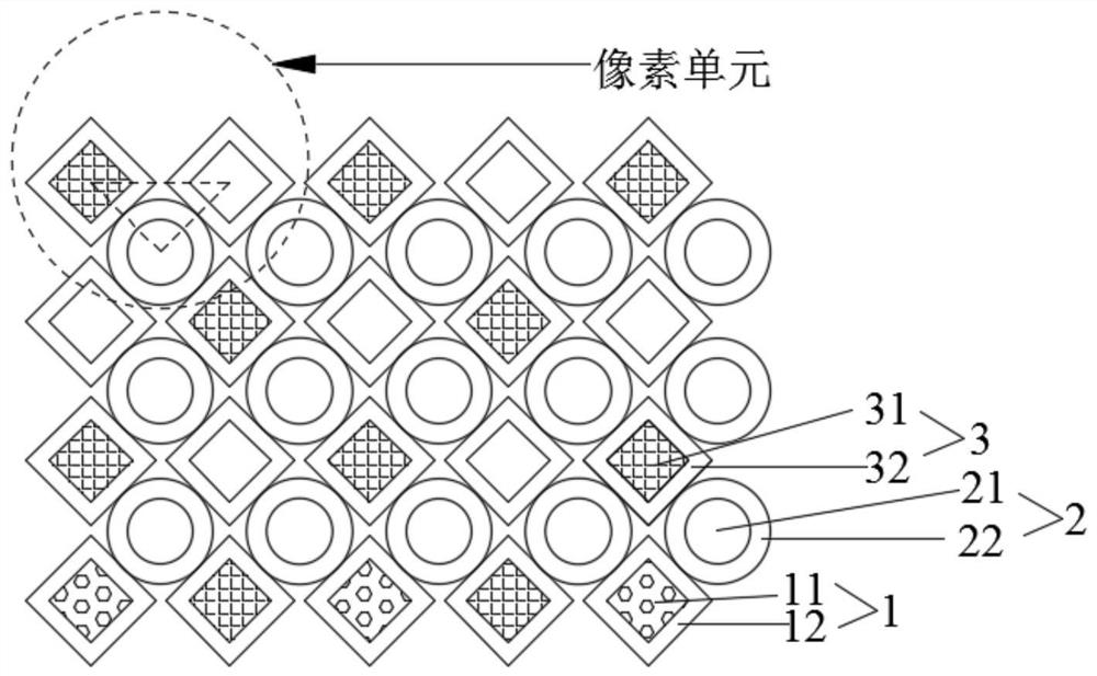
[0038] As mentioned in the background art, users have higher and higher requirements on display clarity and service life of display panels. figure 1 Shown is a schematic diagram of a Diamond pixel structure provided in the prior art. Such as figure 1 As shown, there are light-emitting areas (11, 21, 31 in the figure) and non-light-emitting areas (12, 22, 32 in the figure) in each sub-pixel unit, wherein the non-light-emitting areas (12, 22, 32 in the figure) are composed of pixels The design margin reserved in the manufacturing process. Due to the existence of design margin, fixed screen size, pixel aperture ratio and PPI are negatively correlated, the larger the PPI, the smaller the aperture ratio, and the smaller the PPI, the larger the aperture ratio. The larger the PPI, the higher the clarity, and the larger the aperture ratio, the higher the light extraction efficiency. Fixed screen size, the same PPI requirement, the same luminous flux requirement, the smaller the ape...
PUM
 Abstract
Description
Claims
Application Information
 - R&D
- Intellectual Property
- Life Sciences
- Materials
- Tech Scout
- Unparalleled Data Quality
- Higher Quality Content
- 60% Fewer Hallucinations
Browse by: Latest US Patents, China's latest patents, Technical Efficacy Thesaurus, Application Domain, Technology Topic, Popular Technical Reports.
© 2025 PatSnap. All rights reserved.Legal|Privacy policy|Modern Slavery Act Transparency Statement|Sitemap|About US| Contact US: help@patsnap.com


