Fingerprint recognition assembly, electronic equipment and fingerprint recognition method
A technology of fingerprint identification and components, which is applied in the direction of acquiring/arranging fingerprints/palmprints, character and pattern recognition, computer components, etc., and can solve the problems of poor security and low reliability of fingerprint identification
- Summary
- Abstract
- Description
- Claims
- Application Information
AI Technical Summary
Problems solved by technology
Method used
Image
Examples
Embodiment 1
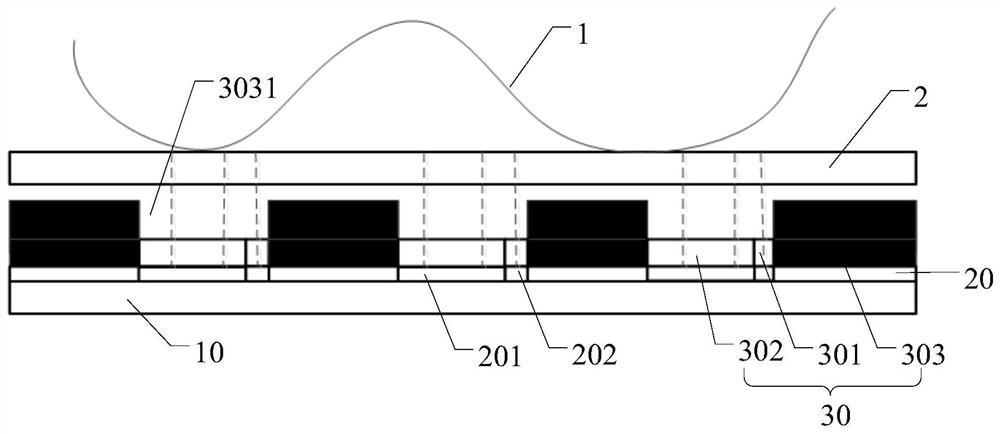
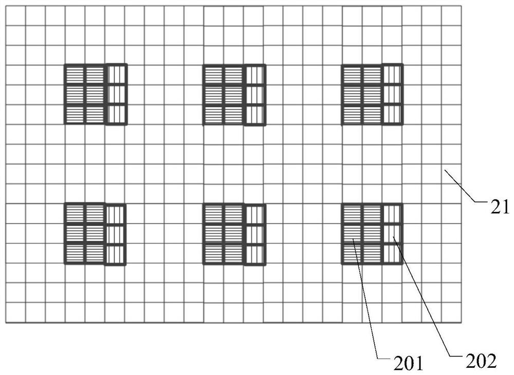
[0034] refer to figure 1 , shows one of the schematic structural diagrams of the fingerprint identification component provided by the embodiment of the present invention. Such as figure 1 As shown, the fingerprint identification component of the embodiment of the present application may specifically include: a substrate 10; a photosensitive layer 20, the photosensitive layer 20 is arranged on the substrate 10, and the photosensitive layer 20 includes: a visible light receiving area 201 and at least one infrared light receiving area 202, visible light The receiving area 201 is used to receive visible light signals, and the infrared light receiving area 202 is used to receive infrared light signals; the optical signal guiding structure 30, the optical signal guiding structure 30 is arranged above the photosensitive layer 20, and the optical signal guiding structure 30 includes: visible light filtering The film layer 301 and the infrared light filter film layer 302; wherein, the...
Embodiment 2
[0050] In this embodiment, the structure and principle of fingerprint identification and biometric identification performed by the fingerprint identification component have been described in detail in Embodiment 1, and will not be repeated here. The embodiment of the present application only elaborates on the structures and principles different from those in the first embodiment in detail.
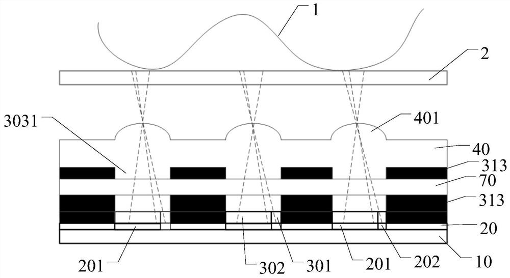
[0051] refer to image 3 , shows the second structural schematic diagram of the fingerprint identification component provided by the embodiment of the present invention. Such as image 3 As shown, the aperture layer 303 includes a plurality of sub-aperture layers 313 stacked; the visible light filter layer 301 and the infrared filter layer 302 are disposed in the aperture 3031 of at least one sub-aperture layer 313 .
[0052] In the embodiment of the present application, in order to improve the guidance of the optical signal carrying the fingerprint information by the aperture layer 303 ...
Embodiment 3
[0095] The embodiment of the present application also provides an electronic device, and the electronic device may specifically include: a display panel and the above-mentioned fingerprint identification component; the fingerprint identification component is disposed under the display panel.
[0096] The electronic device described in the embodiment of the present application may be a smart phone, a computer, a multimedia player, an e-reader, a wearable device, and the like.
[0097] In the embodiment of the present application, since the visible light filter layer is opposite to the infrared light receiving area, the visible light filter layer is used to filter out visible light signals and pass through the infrared light signals; the infrared light The filter film layer is opposite to the visible light receiving area, and the infrared light filter film layer is used to filter out infrared light signals and pass through the visible light signals. Therefore, in practical applic...
PUM
 Abstract
Description
Claims
Application Information
 - R&D
- Intellectual Property
- Life Sciences
- Materials
- Tech Scout
- Unparalleled Data Quality
- Higher Quality Content
- 60% Fewer Hallucinations
Browse by: Latest US Patents, China's latest patents, Technical Efficacy Thesaurus, Application Domain, Technology Topic, Popular Technical Reports.
© 2025 PatSnap. All rights reserved.Legal|Privacy policy|Modern Slavery Act Transparency Statement|Sitemap|About US| Contact US: help@patsnap.com


