High-density trench device structure and manufacturing method thereof

A technology of device structure and manufacturing method, applied in semiconductor/solid-state device manufacturing, semiconductor devices, electrical components, etc., can solve problems such as limiting cell size, simplify the overall structure, increase cell density, and reduce device characteristic conduction The effect of resistance

Pending Publication Date: 2020-10-13
SHANGHAI CHANGYUAN WAYON MICROELECTRONICS
View PDF0 Cites 0 Cited by
  • Summary
  • Abstract
  • Description
  • Claims
  • Application Information

AI Technical Summary

Problems solved by technology

[0006] Aiming at the problem that the existing trench MOSFET structure limits the cell size, a high-density trench device structure and its manufacturing method aimed at effectively increasing the cell density are provided

Method used


Image

  • High-density trench device structure and manufacturing method thereof
  • High-density trench device structure and manufacturing method thereof
  • High-density trench device structure and manufacturing method thereof

Examples


Embodiment 1

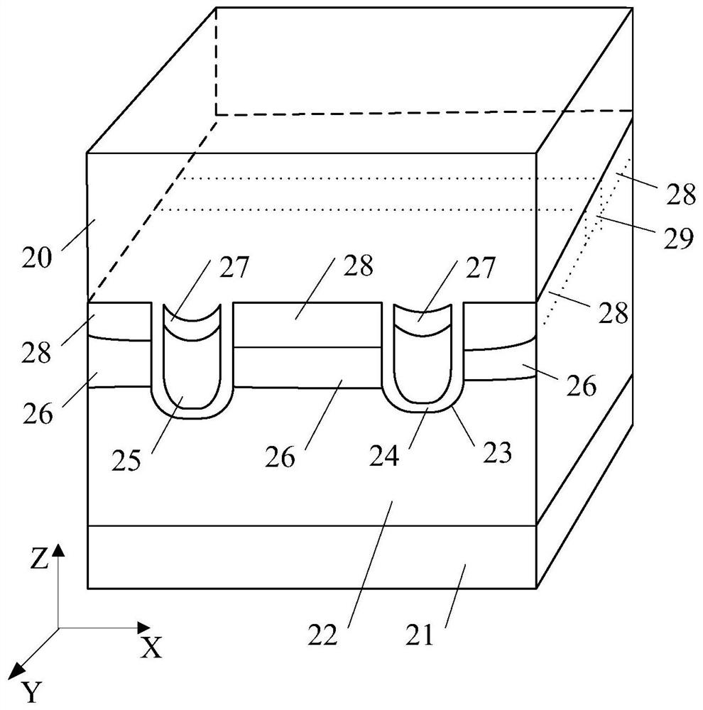
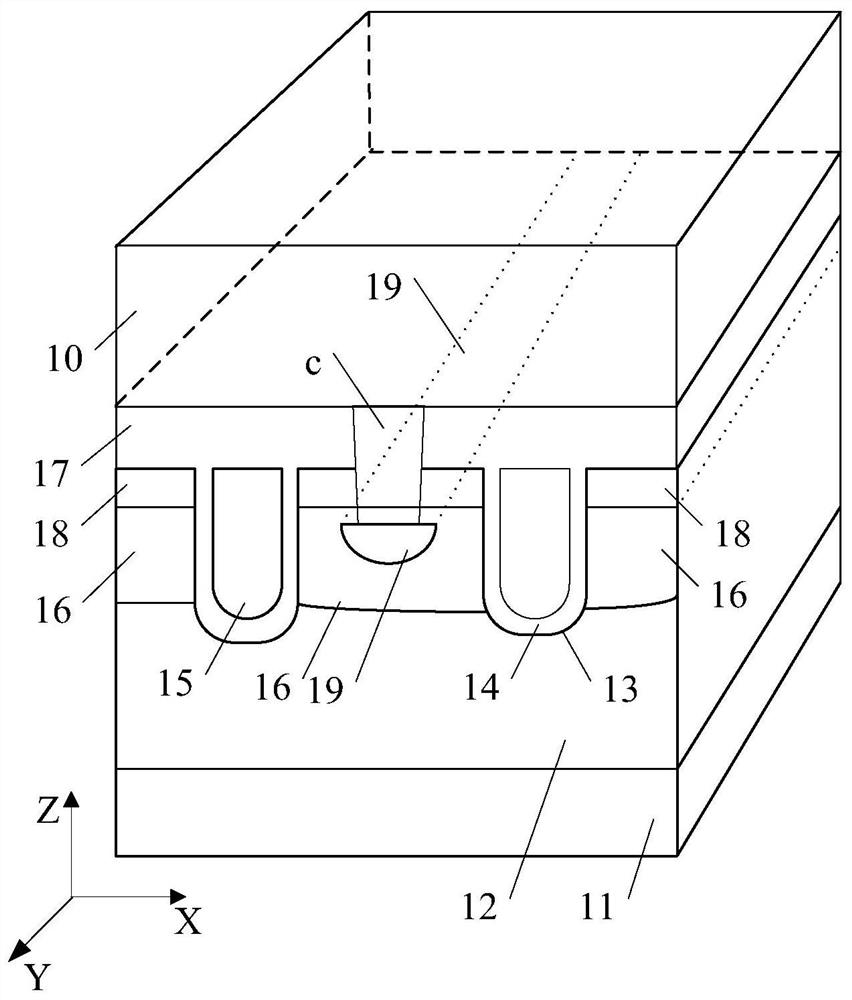
[0053] refer to figure 1 , Figure 3A-Figure 3H As shown, this embodiment provides a high-density trench device structure, including: a substrate 21 of the first conductivity type;

[0054] An epitaxial layer 22 of the first conductivity type located above the substrate 21;

[0055] a plurality of source regions of the first conductivity type formed along the X-axis direction and located above the base region at intervals in the Y-axis direction;

[0056] a base region 26 located above the epitaxial layer 22 and having a second conductivity type;

[0057] Also includes:

[0058] The trench 23 is also lined with an isolation layer 27, and the isolation layer 27 is located above the gate 25;

[0059] A plurality of source regions 28 of the first conductivity type located above the base region 26 are distributed at intervals along the X-axis direction;

[0060] a second conductivity type source region 29 located above the base region 26 and in a spacer region of the first con...

Embodiment 2

[0076] refer to figure 1 , Figure 3A-Figure 3H As shown, among them, Figure 3A-Figure 3H The manufacturing method and process of the high-density trench device structure of this embodiment will be described. This embodiment provides a method for manufacturing a high-density trench device structure, including:

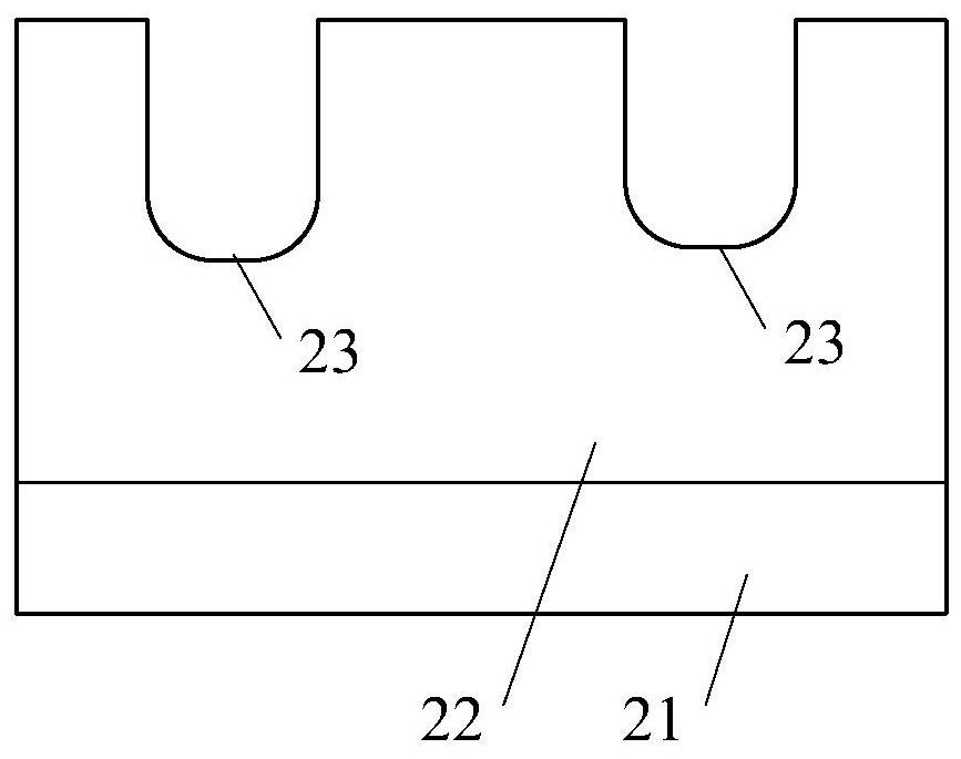
[0077] S1. Form the epitaxial layer 22 of the first conductivity type on the substrate 21 of the first conductivity type (see Figure 3A );

[0078] Wherein, the thickness of the epitaxial layer 22 is 1um˜5um. In practical applications, the thickness of the epitaxial layer 22 can be set according to the withstand voltage requirements of the device.

[0079] S2. Etching trenches 23 in the epitaxial layer 22 along the Y-axis direction (see Figure 3A );

[0080] Specifically, the groove 23 is etched along the Y-axis direction on the epitaxial layer 22 , the etching depth of the groove 23 is 1 um-2 um, the width is 0.2 um-0.7 um, and the groove distance is greate...


PUM

PropertyMeasurementUnit
Thicknessaaaaaaaaaa
Depthaaaaaaaaaa
Widthaaaaaaaaaa

Abstract

The invention discloses a high-density trench device structure and a manufacturing method thereof, and belongs to the field of power semiconductors. According to the high-density trench device structure, an isolation layer sinks into a trench, the whole trench device structure serves as a source region electrode layer, the etching of a source electrode contact hole is not needed, and the whole structure is simplified compared with a traditional trench MOSFET structure; the layout mode that first conductive type source regions and second conductive type source regions are arranged at intervalsin a Y-axis direction is adopted, and the limitation of distribution of the first conductive type source regions and the second conductive type source regions in a transverse direction on the size ofa cellular region is broken through. With the manufacturing method of the high-density groove device structure adopted, the production and manufacturing of an ultra-high-density groove MOSFET with thecell density of 0.5 micrometer or below can be conducted, the cell density is improved by three times or above, and the characteristic on resistance of the device can be reduced by 20% or above on the whole.

Description

technical field [0001] The invention relates to the field of power semiconductors, in particular to a high-density trench device structure and a manufacturing method thereof. Background technique [0002] Trench power MOSFET (Trench MOS) has low switching loss and fast The switching speed is widely used in the field of low-voltage power, such as power management, battery protection and power devices and other application scenarios. [0003] An important index to measure power MOSFET is the characteristic on-resistance Rsp, which is the on-resistance per unit area of ​​the chip; the device on-resistance is usually composed of substrate resistance, epitaxial layer resistance, channel resistance, source-drain level contact resistance, etc. , for low-voltage MOSFETs, the channel resistance accounts for about 1 / 3 of the device resistance. At present, an important measure to reduce the on-resistance of power devices is to increase the cell density, that is, to have a higher numb...

Claims


Application Information

Patent Timeline
IPC IPC(8): H01L29/06H01L29/423H01L29/78H01L21/336H01L21/28
CPCH01L29/0642H01L29/0684H01L29/0696H01L29/401H01L29/42356H01L29/4236H01L29/66666H01L29/7827
Inventor 苏亚兵马一洁何鑫鑫
Owner SHANGHAI CHANGYUAN WAYON MICROELECTRONICS
Why Eureka
Try Eureka