Image processing method and system, medium, chip and structural optoelectronic equipment
An image processing and optoelectronic technology, applied in the field of image processing, can solve problems such as reducing system performance and image acquisition and processing efficiency, and achieve the effect of improving processing efficiency, reducing workload, and optimal system performance
- Summary
- Abstract
- Description
- Claims
- Application Information
AI Technical Summary
Problems solved by technology
Method used
Image
Examples
Embodiment 1
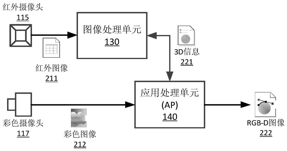
[0075] Such as image 3 As shown, in this embodiment, the image processing unit 130 sends a shooting instruction to the infrared camera 115; the infrared camera 115 acquires an infrared image 211 of a 3D object according to the received shooting instruction, and sends the infrared image 211 is sent to the image processing unit 130. The image processing unit 130 performs image processing on the infrared image 211 , acquires 3D information 221 of the infrared image 211 , and sends the 3D information 221 to the application processing unit 140 through a data line.
[0076] The application processing unit 140 sends a shooting instruction to the color camera 117, and the color camera 117 acquires a color image 212 of a 3D object according to the received shooting instruction, and sends the color image 212 to the application processing unit 140 .
[0077] The application processing unit 140 performs processing according to the received 3D information 221 and the color image 212, th...
Embodiment 2
[0080] Such as Figure 4 As shown, in this embodiment, the application processing module 140 sends a shooting instruction to the infrared camera 115 and the color camera 117 . The infrared camera 115 acquires an infrared image 231 of a 3D object according to the received shooting instruction, and sends the infrared image 231 to the application processing unit 140 . The color camera 117 acquires a color image 232 of a 3D object according to the received shooting instruction, and sends the color image 232 to the application processing unit 140 .
[0081] . The application processing unit 140 sends the received infrared image 231 (or color image 232) to the image processing unit 130; the image processing unit 130 images the infrared image 231 (or color image 232) processing to obtain 3D information 241 of the infrared image 231 , and send the 3D information 241 to the application processing unit 140 through a data line.
[0082] The application processing unit 140 performs proc...
Embodiment 3
[0085] Such as Figure 5 As shown, in this embodiment, the image processing unit 130 sends a shooting instruction to the infrared camera 115 and the color camera 117 . The infrared camera 115 acquires an infrared image 251 of a 3D object according to the received shooting instruction, and sends the infrared image 251 to the image processing unit 130 . The color camera 117 acquires a color image 252 of a 3D object according to the received shooting instruction, and sends the color image 252 to the image processing unit 130 .
[0086]The image processing unit 130 performs image processing on the infrared image 251 , acquires 3D information 261 , and sends the 3D information 261 and the color image 252 to the application processing unit 140 .
[0087] The application processing unit 140 performs processing according to the received 3D information 261 and the color image 252, thereby obtaining the RGB-D image 262 of the infrared image 251 and the color image 252, which helps real...
PUM
 Abstract
Description
Claims
Application Information
 - R&D Engineer
- R&D Manager
- IP Professional
- Industry Leading Data Capabilities
- Powerful AI technology
- Patent DNA Extraction
Browse by: Latest US Patents, China's latest patents, Technical Efficacy Thesaurus, Application Domain, Technology Topic, Popular Technical Reports.
© 2024 PatSnap. All rights reserved.Legal|Privacy policy|Modern Slavery Act Transparency Statement|Sitemap|About US| Contact US: help@patsnap.com


