Display module and display device
A technology of display module and display area, which is applied in semiconductor/solid-state device parts, instruments, sub-office equipment, etc.
- Summary
- Abstract
- Description
- Claims
- Application Information
AI Technical Summary
Problems solved by technology
Method used
Image
Examples
Embodiment Construction
[0022] Embodiments of the present invention are described in detail below. The embodiments described below are exemplary only for explaining the present invention and should not be construed as limiting the present invention. If no specific technique or condition is indicated in the examples, it shall be carried out according to the technique or condition described in the literature in this field or according to the product specification.
[0023] The present invention is based on the following discoveries and recognitions of the inventors:
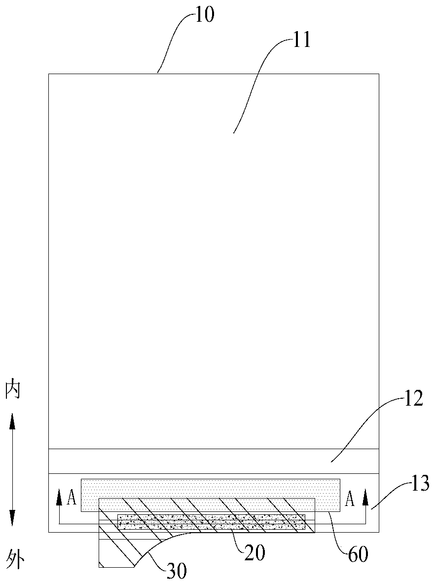
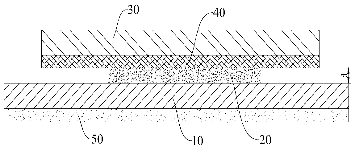
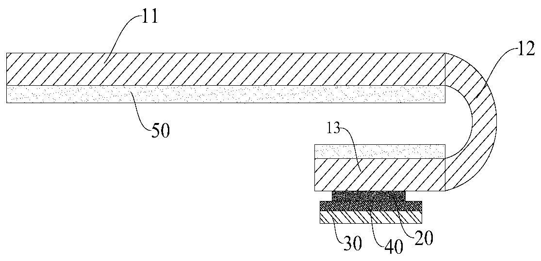
[0024] Although the COP packaging technology can make the frame very narrow, it also brings problems such as low yield rate, local overheating and causing Panel burning and signal interference. Among them, the local overheating problem is because the driver IC of the COP packaging technology is installed with the front facing up, the back is the panel substrate, and the lower part of the substrate is the SCF (heat dissipation film), so t...
PUM
| Property | Measurement | Unit |
|---|---|---|
| Thickness | aaaaa | aaaaa |
Abstract
Description
Claims
Application Information
 - R&D Engineer
- R&D Manager
- IP Professional
- Industry Leading Data Capabilities
- Powerful AI technology
- Patent DNA Extraction
Browse by: Latest US Patents, China's latest patents, Technical Efficacy Thesaurus, Application Domain, Technology Topic, Popular Technical Reports.
© 2024 PatSnap. All rights reserved.Legal|Privacy policy|Modern Slavery Act Transparency Statement|Sitemap|About US| Contact US: help@patsnap.com


