3d NAND memory and its formation method

A 3D NAND and memory technology, which is applied in semiconductor devices, electrical solid devices, electrical components, etc., can solve problems such as storage structure breakage and storage structure failure, and achieve the effect of reducing difficulty and simplifying process steps

Active Publication Date: 2021-05-18
YANGTZE MEMORY TECH CO LTD
View PDF6 Cites 0 Cited by
  • Summary
  • Abstract
  • Description
  • Claims
  • Application Information

AI Technical Summary

Problems solved by technology

[0005] The technical problem to be solved by the present invention is that the storage structure formed in the channel hole is prone to defects such as fracture, which makes the storage structure invalid and simplifies the manufacturing process.

Method used


Image

  • 3d NAND memory and its formation method
  • 3d NAND memory and its formation method
  • 3d NAND memory and its formation method

Examples


Embodiment Construction

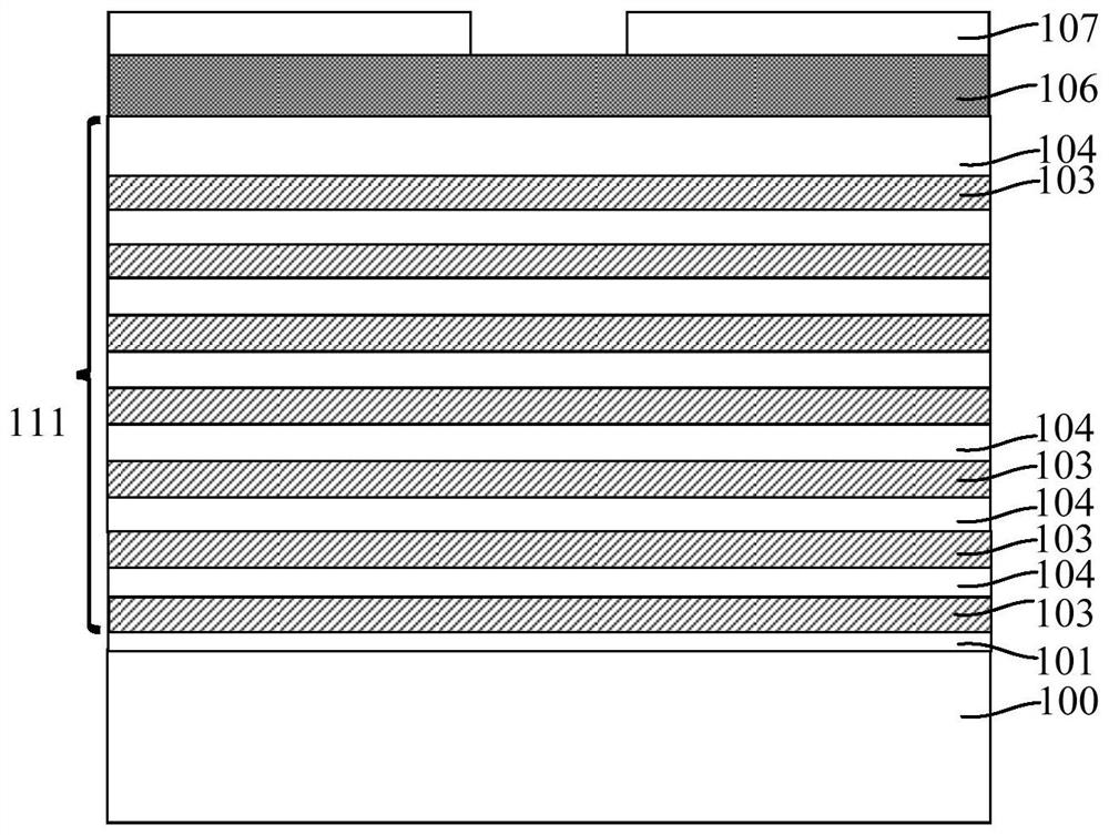
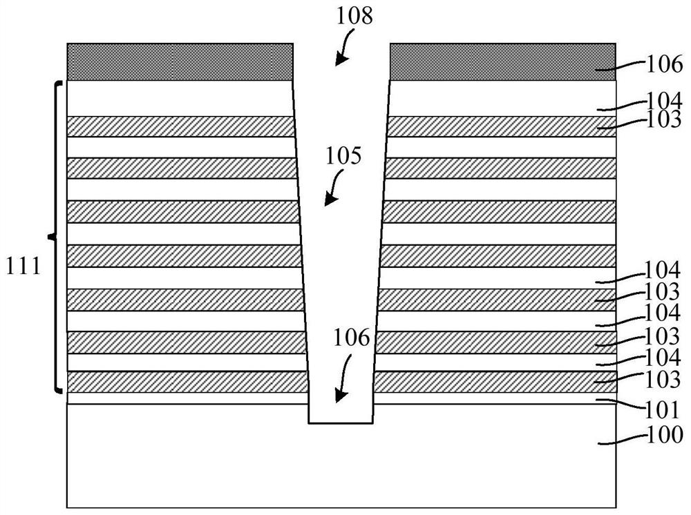
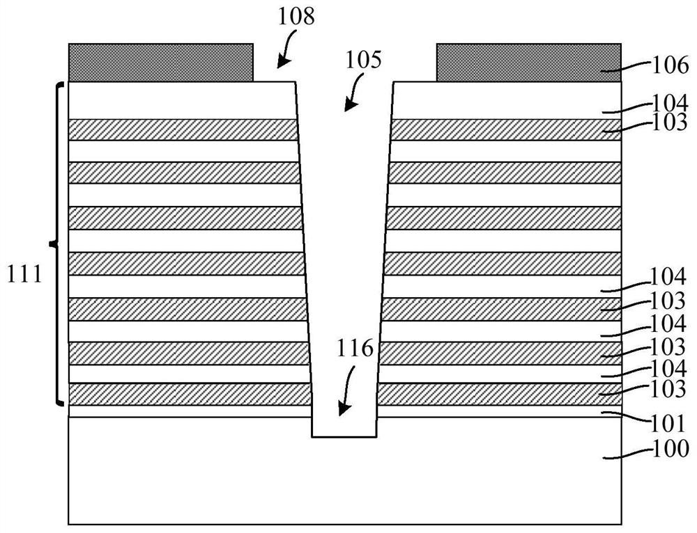
[0033] As mentioned in the background, the existing 3D NAND memory with a multilayer stack structure has the problem that the position of the channel hole formed in the upper layer stack structure and the channel hole formed in the lower layer stack structure are offset. When the upper and lower channel holes are formed When the position is shifted, the difficulty of the storage structure formed in the channel hole will increase, and the storage structure formed in the channel hole will easily produce defects such as fractures (when the position of the upper and lower channel holes is offset, the upper channel hole The bottom part is located on the surface of the stacked structure below, and laterally extending steps are formed on the side walls of the channel holes connected up and down. The existence of the steps makes it easy for the charge storage layer in the storage structure to be cut off at the steps when the storage structure is formed. ), making the storage structure ...


PUM


Abstract

A 3D NAND memory and its forming method. In the forming method, before the sacrificial layer is filled in the first channel hole, a hole expansion step is performed to increase the width of the opening of the first channel hole. Through the hole expansion step, the width of the opening of the first channel hole is increased, and the second stack structure is subsequently formed on the first stack structure, even if the position of the second channel hole formed in the second stack structure is relative to the first There is a certain positional offset of the channel hole, and the bottom position of the second channel hole can still fall in the widened opening of the first channel hole, which reduces the gap between the first channel hole and the second channel hole. It is difficult to form the memory structure, and since the hole expansion step is performed before filling the sacrificial layer in the first channel hole, only one step of filling the sacrificial layer is required before forming the second stacked structure, which simplifies the process steps.

Description

technical field [0001] The invention relates to the field of semiconductor manufacturing, in particular to a 3D NAND memory and a forming method thereof. Background technique [0002] NAND flash memory is a better storage device than hard disk drives, and it has been widely used in electronic products as people pursue non-volatile storage products with low power consumption, light weight and high performance. At present, the NAND flash memory with a planar structure is close to the limit of practical expansion. In order to further increase the storage capacity and reduce the storage cost per bit, a 3D NAND memory with a 3D structure is proposed. [0003] The formation process of the existing 3D NAND memory generally includes: forming a stacked layer in which silicon nitride layers and silicon oxide layers are alternately stacked on a substrate; etching the stacked layer to form channel holes in the stacked layer; After the hole, the substrate at the bottom of the channel ho...

Claims


Application Information

Patent Timeline
Patent Type & Authority Patents(China)
IPC IPC(8): H01L27/1157H01L27/11582
CPCH10B43/35H10B43/27
Inventor 董明曾凡清
Owner YANGTZE MEMORY TECH CO LTD
Why Eureka
Try Eureka