Explosion-proof PCB
A kind of PCB board, explosion-proof technology, applied in printed circuit components, circuit thermal devices, printed circuit stress/deformation reduction and other directions, can solve problems such as damage and explosion of PCB boards, prolong service life, reduce production costs, and prevent deformation. Effect
- Summary
- Abstract
- Description
- Claims
- Application Information
AI Technical Summary
Problems solved by technology
Method used
Image
Examples
Embodiment 1
[0026] The embodiment of the invention discloses an explosion-proof PCB board,
[0027] Specifically include:
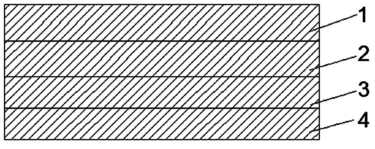
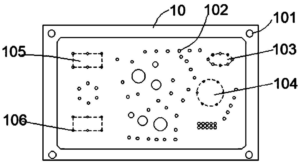
[0028] see figure 1 , figure 2 , an explosion-proof PCB board, including a top board 1, a wire layer 2, a signal layer 3 and a bottom board 4 connected in sequence, the top board 1, the wire layer 2, the signal layer 3 and the bottom board 4 have the same structure, each The layers are bonded with an insulating bonding material, and the top layer board 1 is a PCB substrate 10;
[0029] The PCB substrate 10 includes a mounting hole 101, a circuit connection pad 102, an oval mounting area 103, a circular mounting area 104, a rectangular mounting area 105 and an explosion-proof hole 106;
[0030] The bottom of the bottom plate 4 is provided with a layer of natural graphite heat dissipation film.
[0031] The explosion-proof PCB board is formed by laminating a top layer board 1 , a wire layer 2 , a signal layer 3 and a bottom board 4 .
[0032] The PCB substrate 10...
Embodiment 2
[0043] The embodiment of the invention discloses an explosion-proof PCB board,
[0044] Specifically include:
[0045] see figure 1 , figure 2 , an explosion-proof PCB board, including a top board 1, a wire layer 2, a signal layer 3 and a bottom board 4 connected in sequence, the top board 1, the wire layer 2, the signal layer 3 and the bottom board 4 have the same structure, each The layers are bonded with an insulating bonding material, and the top layer board 1 is a PCB substrate 10;
[0046] The PCB substrate 10 includes a mounting hole 101, a circuit connection pad 102, an oval mounting area 103, a circular mounting area 104, a rectangular mounting area 105 and an explosion-proof hole 106;
[0047] The bottom of the bottom plate 4 is provided with a layer of artificial graphite heat dissipation film.
[0048] The explosion-proof PCB board is formed by laminating a top layer board 1 , a wire layer 2 , a signal layer 3 and a bottom board 4 .
[0049] The PCB substrate...
Embodiment 3
[0060] The embodiment of the invention discloses an explosion-proof PCB board,
[0061] Specifically include:
[0062] see figure 1 , figure 2 , an explosion-proof PCB board, including a top board 1, a wire layer 2, a signal layer 3 and a bottom board 4 connected in sequence, the top board 1, the wire layer 2, the signal layer 3 and the bottom board 4 have the same structure, each The layers are bonded with an insulating bonding material, and the top layer board 1 is a PCB substrate 10;
[0063] The PCB substrate 10 includes a mounting hole 101, a circuit connection pad 102, an oval mounting area 103, a circular mounting area 104, a rectangular mounting area 105 and an explosion-proof hole 106;
[0064] A layer of nano-carbon heat dissipation film is provided on the bottom of the bottom plate 4 .
[0065] The explosion-proof PCB board is formed by laminating a top layer board 1 , a wire layer 2 , a signal layer 3 and a bottom board 4 .
[0066] The PCB substrate 10 is pr...
PUM
 Abstract
Description
Claims
Application Information
 - R&D Engineer
- R&D Manager
- IP Professional
- Industry Leading Data Capabilities
- Powerful AI technology
- Patent DNA Extraction
Browse by: Latest US Patents, China's latest patents, Technical Efficacy Thesaurus, Application Domain, Technology Topic, Popular Technical Reports.
© 2024 PatSnap. All rights reserved.Legal|Privacy policy|Modern Slavery Act Transparency Statement|Sitemap|About US| Contact US: help@patsnap.com


