Integrated structure of crystal resonator and control circuit and integration method thereof
A crystal resonator and control circuit technology, which is applied in semiconductor/solid-state device manufacturing, circuits, electric solid-state devices, etc., can solve the problems of large size and difficult integration, and achieve the effect of small size and improved integration.
- Summary
- Abstract
- Description
- Claims
- Application Information
AI Technical Summary
Problems solved by technology
Method used
Image


Examples
Embodiment 1
[0045] Figure 2a ~ Figure 2g It is a structural schematic diagram of the integration method of the crystal resonator and the control circuit in the first embodiment of the present invention during its preparation process. Each step in this embodiment will be described in detail below with reference to the accompanying drawings.
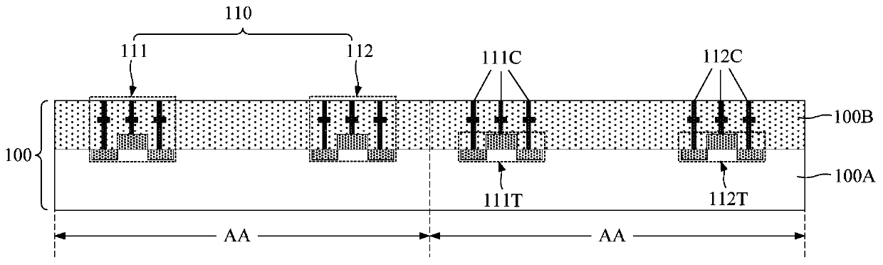
[0046] In step S100, specifically refer to Figure 2a and Figure 2b As shown, a device wafer 100 is provided, in which a control circuit 110 is formed, and the device wafer 100 is etched to form a lower cavity 120 of the crystal resonator. That is, the lower cavity 120 is exposed from the front surface of the device wafer 100 , and the control circuit 110 is used, for example, to apply electrical signals to both sides of the piezoelectric wafer formed subsequently.
[0047] Wherein, a plurality of crystal resonators can be prepared simultaneously on the same device wafer 100, so a plurality of device areas AA are correspondingly defined on the de...
Embodiment 2
[0095] The difference from Embodiment 1 is that in this embodiment, the upper electrode 230, the piezoelectric wafer 220 and the lower electrode 210 of the piezoelectric resonator plate 200 are all formed on the front surface of the device wafer 100, and the The piezoelectric resonator plate 200 covers the opening of the lower cavity 120, and the formed crystal resonator is electrically connected to the control circuit in the device wafer 100, and then the bonding process is performed so that the upper cavity 310 corresponds to the The side of the piezoelectric resonator plate 200 facing away from the lower cavity 120 constitutes a crystal resonator, thereby realizing the integrated arrangement of the crystal resonator and the control circuit.
[0096] Specifically, in step S300, the method for forming the piezoelectric resonant plate on the device wafer 100 includes:
[0097] First, a lower electrode 210 is formed at a set position on the surface of the device wafer 100; in t...
Embodiment 3
[0111] In Embodiment 1 and Embodiment 2, the piezoelectric resonant plates including the upper electrode, the piezoelectric wafer and the lower electrode are all formed on the substrate or the device wafer. The difference from the above embodiment is that in this embodiment, the upper electrode and the piezoelectric wafer are formed on the substrate, and the lower electrode is formed on the device wafer.
[0112] Figure 3a ~ Figure 3e It is a schematic structural diagram of the method for integrating the crystal resonator and the control circuit in the third embodiment of the present invention during its preparation process. The steps of forming the crystal resonator in this embodiment will be described in detail below with reference to the accompanying drawings.
[0113] In step S100 and step S300, focus on referring to Figure 3a As shown, a device wafer 100 is provided, and a control circuit is formed in the device wafer 100, and a lower electrode 210 is formed on the sur...
PUM
 Abstract
Description
Claims
Application Information
 - Generate Ideas
- Intellectual Property
- Life Sciences
- Materials
- Tech Scout
- Unparalleled Data Quality
- Higher Quality Content
- 60% Fewer Hallucinations
Browse by: Latest US Patents, China's latest patents, Technical Efficacy Thesaurus, Application Domain, Technology Topic, Popular Technical Reports.
© 2025 PatSnap. All rights reserved.Legal|Privacy policy|Modern Slavery Act Transparency Statement|Sitemap|About US| Contact US: help@patsnap.com