Top-emitting electroluminescent device and manufacturing method thereof

An electroluminescent device and top-emission technology, which is applied in the direction of electric solid-state devices, semiconductor/solid-state device manufacturing, and electrical components, and can solve the problems of increased equipment investment and time-consuming processes

Pending Publication Date: 2020-07-07
GUANGDONG JUHUA PRINTING DISPLAY TECH CO LTD
View PDF0 Cites 0 Cited by
  • Summary
  • Abstract
  • Description
  • Claims
  • Application Information

AI Technical Summary

Problems solved by technology

However, for medium and large-sized top-emitting OLED devices using transparent conductive oxide materials as the cathode, if a layer of CPL needs to be evaporated after the cathode is prepared by the sputtering process, it is necessary to add another one after the sputtering equipment. Evaporation equipment, resulting in increased equipment investment and time-consuming process

Method used


Image

  • Top-emitting electroluminescent device and manufacturing method thereof
  • Top-emitting electroluminescent device and manufacturing method thereof
  • Top-emitting electroluminescent device and manufacturing method thereof

Examples


Embodiment Construction

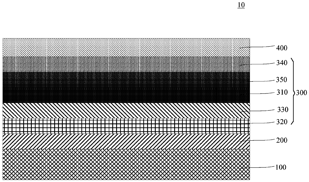
[0028] In order to facilitate the understanding of the present invention, the present invention will be described more fully below with reference to the relevant drawings. The preferred embodiments of the invention are shown in the drawings. However, the present invention can be implemented in many different forms and is not limited to the embodiments described herein. On the contrary, the purpose of providing these embodiments is to make the understanding of the disclosure of the present invention more thorough and comprehensive.

[0029] It should be noted that when an element is referred to as being "disposed on" another element, it can be directly on the other element or a centered element may also exist. When an element is considered to be "connected" to another element, it can be directly connected to the other element or an intermediate element may be present at the same time.

[0030] Unless otherwise defined, all technical and scientific terms used herein have the same m...


PUM

PropertyMeasurementUnit
Thicknessaaaaaaaaaa
Thicknessaaaaaaaaaa
Thicknessaaaaaaaaaa

Abstract

The invention relates to a top-emitting electroluminescent device and a manufacturing method thereof. The device includes a substrate, and a first electrode layer, a light emitting unit layer, and a light extraction second electrode layer stacked on the substrate. According to the top-emitting electroluminescent device, a transparent conductive oxide thin film layer is adopted as the light extraction second electrode layer, so that a CPL layer is unnecessary to be manufactured on the transparent conductive oxide thin film layer through evaporation, and evaporation equipment is unnecessary to be additionally arranged behind sputtering equipment during manufacturing, and thereby, equipment investment is reduced, the process is simplified, production efficiency is improved, and cost is reduced. The light extraction second electrode layer can be used as a light extraction layer for light extraction while playing a role of a conductive electrode, and higher light extraction efficiency can be obtained by adopting a specific thickness range and a specific refractive index range, so that higher device current efficiency is achieved. The light extraction second electrode layer has multiplepurposes, the structure of a device product is simplified, and the ultrathin design of the product is facilitated while the cost is reduced.

Description

Technical field [0001] The present invention relates to the field of electroluminescence technology, in particular to a top emission electroluminescence device and a manufacturing method thereof. Background technique [0002] Due to the advantages of high contrast, wide color gamut, and fast response speed, OLED (organic light-emitting diode) displays are increasingly occupying the market share of high-end display devices. Traditional bottom-emitting OLED devices are limited by the low aperture ratio, which is very challenging to manufacture higher resolution 8K TVs. Therefore, the current development trend of the OLED device structure is toward a top-emitting device structure that can obtain a higher aperture ratio. [0003] For the top-emitting device structure of small-size OLED displays such as mobile phones, a thin layer of metal with higher reflectivity is usually used as a translucent cathode. This cathode will produce a strong microcavity effect, resulting in the viewing a...

Claims


Application Information

Patent Timeline
IPC IPC(8): H01L51/50H01L51/52H01L51/56
CPCH10K50/13H10K50/805H10K71/00
Inventor 李哲宋晶尧付东
Owner GUANGDONG JUHUA PRINTING DISPLAY TECH CO LTD
Why Eureka
Try Eureka