
Twenty-million-pixel small lens

A pixel and lens technology, applied in the field of 20 million pixel small lenses, can solve problems such as insufficient performance

Pending Publication Date: 2020-06-19
FOCTEK PHOTONICS LNC
View PDF0 Cites 0 Cited by
  • Summary
  • Abstract
  • Description
  • Claims
  • Application Information

AI Technical Summary

Problems solved by technology

Conventional high-resolution lenses currently on the market have a resolution of about 4K, that is, about 8 million pixels, and the highest one is about 12 million pixels. Matching with high-resolution chips, the performance is already insufficient

Method used


Image

  • Twenty-million-pixel small lens
  • Twenty-million-pixel small lens
  • Twenty-million-pixel small lens

Examples


Embodiment Construction

[0031] The present invention is described in detail below in conjunction with accompanying drawing description:

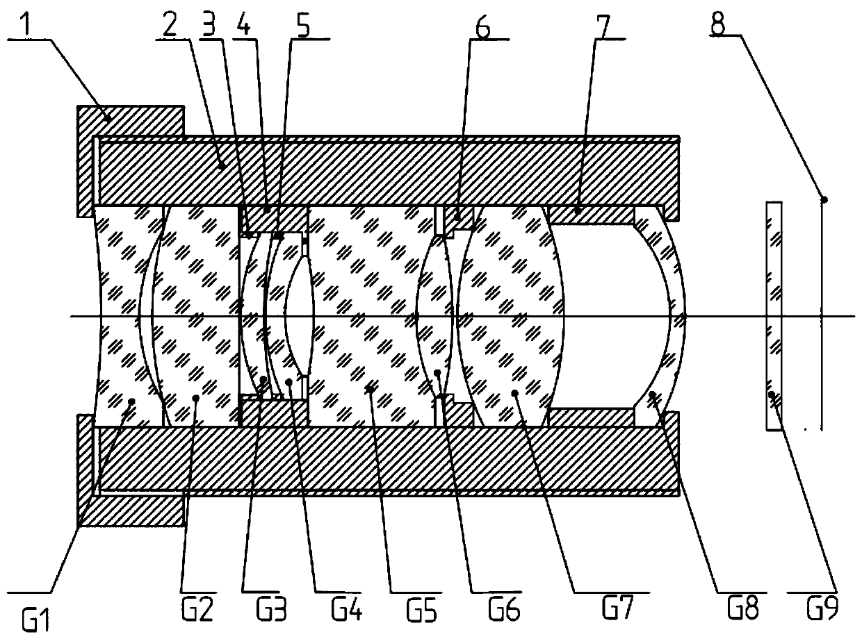
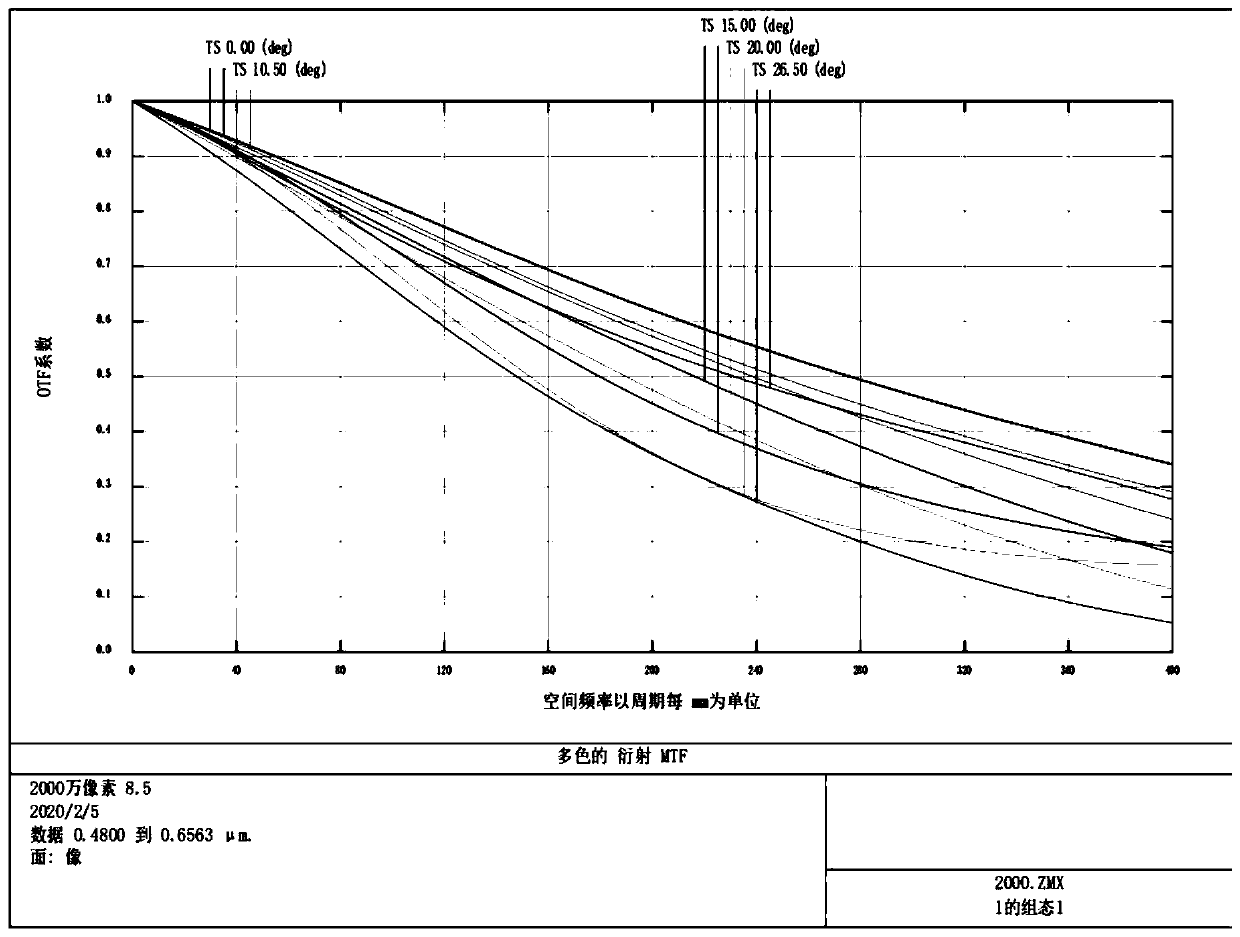
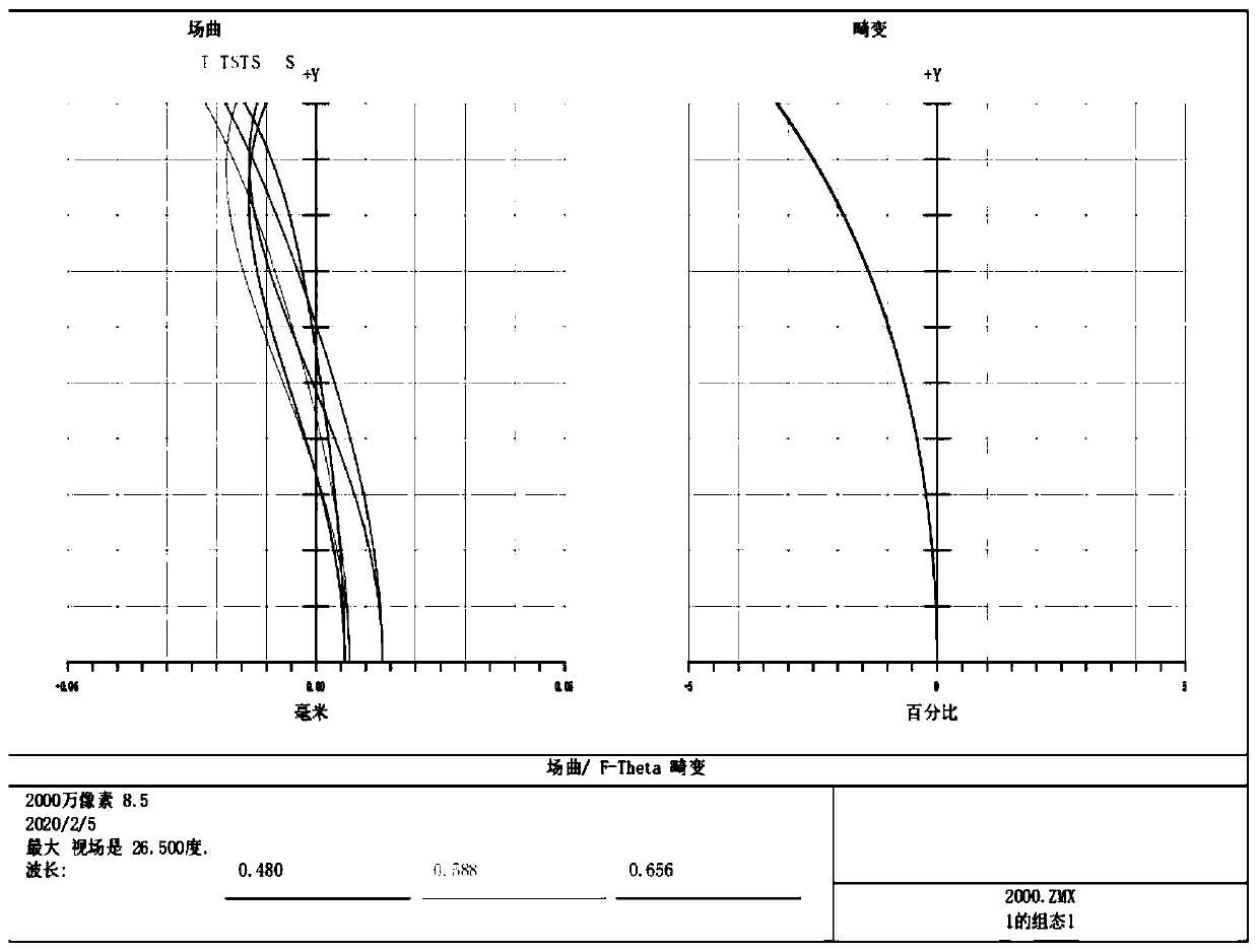
[0032] Such as Figure 1-4 Shown, a kind of 20,000,000 pixel small lens is characterized in that: comprise main lens barrel 2, the front mirror group that is arranged in the main lens barrel 2 successively along the light incident direction, aperture, rear mirror group, and be arranged on the main lens barrel The photosensitive chip 8 at the rear end of the lens barrel 2, the focal length range of the front lens group is -50~-100mm, and the focal length range of the rear lens group is 6~12mm;

[0033] The front lens group includes a first lens G1, a second lens G2, a third lens G3, and a fourth lens G4 arranged in sequence along the light incident direction, and the rear lens group includes a fifth lens G5 arranged in sequence along the light incident direction , the sixth lens G6, the seventh lens G7 and the eighth lens G8;

[0034] The first lens G1 is a biconc...


PUM


Abstract

The invention relates to a twenty-million-pixel small lens which comprises a main lens cone, a front lens group, a diaphragm, a rear lens group and a photosensitive chip arranged at the rear end of the main lens cone, the focal length of the front lens group ranges from -50 mm to 100 mm, and the focal length of the rear lens group ranges from 6 mm to 12 mm. The front lens group comprises a first lens, a second lens and a third lens. The rear lens group comprises a fifth lens, a sixth lens, and a seventh lens and an eighth lens which are biconcave lenses. The second lens is a biconvex lens, thethird lens is a meniscus lens, the fourth lens is a meniscus lens, the fifth lens is a biconcave lens, the sixth lens is a biconvex lens, the seventh lens is a biconvex lens, and the eighth lens is ameniscus lens. The twenty-million-pixel small lens is used for more than 20 million pixels and more than 1 / 2.3 inch imaging target surface of an imaging chip, and has the characteristics of large target surface and high resolution.

Description

technical field [0001] The invention relates to the lens field, in particular to a small lens with 20 million pixels. Background technique [0002] With the rapid development of imaging photosensitive chips, the pixels of imaging chips have made a qualitative leap. High-resolution images have two meanings for observers. One meaning is that under the same spatial resolution (when the space corresponding to each pixel has the same size), high-resolution means that a wider area can be seen. Viewable range. Another meaning is that under the same field of view, high resolution can provide more details. Both CCD and CMOS chips are developing towards high resolution. The methods to improve the resolution are: one is to increase the size of the chip wafer; the other is to reduce the size of the pixel to obtain more image pixels on the same area of ​​the wafer. [0003] The existing CMOS chips on the market have a pixel size of less than 1um and a resolution higher than 20 millio...

Claims


Application Information

Patent Timeline
IPC IPC(8): G02B7/02
CPCG02B7/021
Inventor 黄统樑
Owner FOCTEK PHOTONICS LNC
Learn More