A wafer test probe station

A technology of wafer testing and testing probes, which is applied in the direction of measuring electricity, measuring devices, measuring electrical variables, etc., and can solve problems such as unsuitable wafer fixing and wafer fixing failure

Active Publication Date: 2022-05-03
HANGZHOU HIKMICRO SENSING TECH CO LTD
View PDF15 Cites 1 Cited by
  • Summary
  • Abstract
  • Description
  • Claims
  • Application Information

AI Technical Summary

Problems solved by technology

[0003] In the process of realizing the present invention, the inventor found that the above method of fixing the wafer has the following problems: when in a vacuum test environment, the inside of the suction cup and the external environment are both in a vacuum state, which will cause the wafer to be fixed.
[0004] Therefore, the existing method of fixing wafers by vacuum adsorption is not suitable for fixing wafers in a vacuum test environment.

Method used


Image

  • A wafer test probe station
  • A wafer test probe station
  • A wafer test probe station

Examples


Embodiment 1

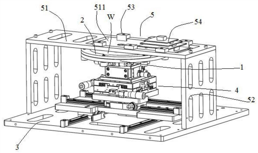
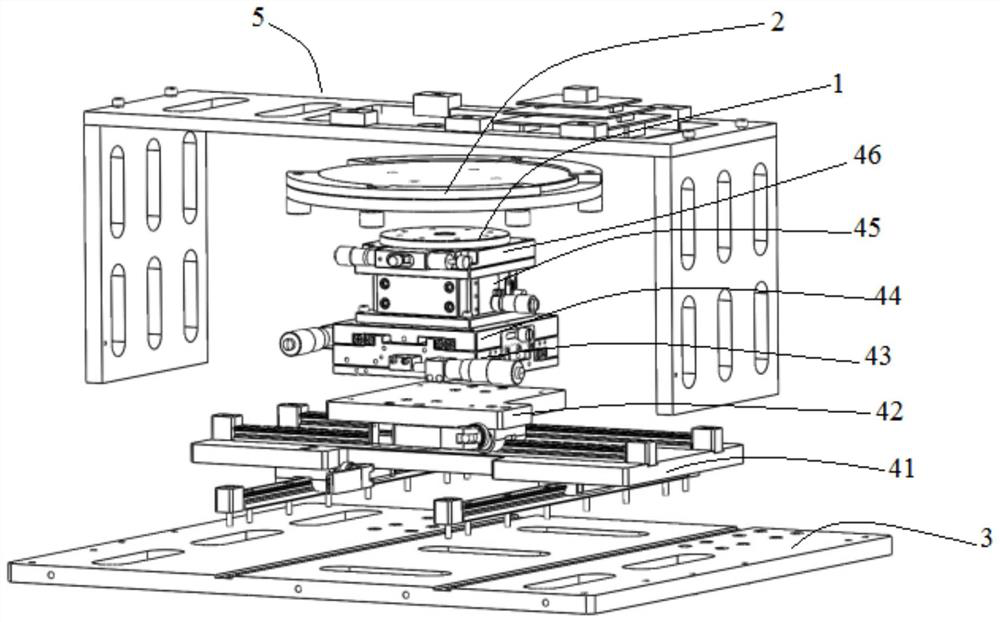
[0041] see Figure 1 to Figure 3 As shown, an embodiment of the present invention provides a wafer testing probe station, which is mainly used in performance testing of semiconductors, optoelectronic components, integrated circuits, etc., especially for testing wafers; It refers to the silicon wafer used in the manufacture of silicon semiconductor integrated circuits. Because of its circular shape, it is called a wafer. The probe station includes a stage 1 on which a pressing ring 2 for fixing the wafer W is provided, and a structure corresponding to the outline of the wafer is provided on the pressing ring.

[0042] In this embodiment, the term “correspondence” refers to the same contour, which can be installed or fixed with each other in structure. For example, the contour of the wafer is circular. Correspondingly, the pressure ring is provided with an arc or circular structure. features to fit the wafer profile and hold the wafer in place.

[0043] According to an embodim...


PUM


Abstract

The embodiment of the invention discloses a wafer testing probe station, which relates to the technical field of silicon wafer testing and is applicable to fixing wafers in a vacuum testing environment. It includes: a carrier platform, on which a pressure ring for fixing the wafer is arranged, and a structure corresponding to the outline of the wafer is arranged on the pressure ring. The invention is suitable for performance testing of semiconductors, photoelectric components, integrated circuits, etc., and is especially suitable for testing wafers.

Description

technical field [0001] The invention relates to the technical field of silicon wafer testing, in particular to a wafer testing probe station. Background technique [0002] At present, when the wafer is tested under standard atmospheric pressure, the method of vacuum adsorption and fixation of the wafer is usually adopted. When it is working, a pressure vacuum state is formed inside the suction cup, which is lower than the external atmospheric pressure. The workpiece, such as a wafer, is adsorbed and fixed under the action of external pressure. The higher the vacuum degree inside the suction cup, the tighter the suction and fixation between the two. [0003] In the process of realizing the present invention, the inventor found that the above-mentioned method of fixing the wafer has the following problems: when in a vacuum test environment, the inside of the suction cup and the external environment where it is located are in a vacuum state, which will cause the wafer fixing fa...

Claims


Application Information

Patent Timeline
Patent Type & Authority Patents(China)
IPC IPC(8): G01R1/073
CPCG01R1/07342
Inventor 刘旭峰
Owner HANGZHOU HIKMICRO SENSING TECH CO LTD
Why Eureka
Try Eureka