Integrated wide-narrow ridge waveguide and manufacturingprocess thereof
A preparation process and technology of ridge waveguides, which are applied in the directions of waveguides, waveguide-type devices, circuits, etc., to achieve the effect of improving accuracy
- Summary
- Abstract
- Description
- Claims
- Application Information
AI Technical Summary
Problems solved by technology
Method used
Image
Examples
Embodiment Construction
[0032] The technical solution of the present invention will be further described in detail below in conjunction with specific examples, but the protection scope of the present invention is not limited to the following description.
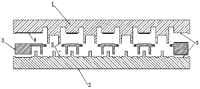
[0033] Such as figure 2 As shown, an integrated wide and narrow ridge waveguide includes an upper cavity 1, a lower cavity 2 and a plurality of middle cavities 3. A waveguide cavity is formed between the upper cavity 1 and the lower cavity 2. The structure of the waveguide cavity can refer to Figure 6 shown. The middle cavity body 3 is evenly distributed among the waveguide cavities, and divides the waveguide cavity into alternating wide-side ridge waveguides 6 and narrow-wave ridge waveguides 7. Its structure is as follows image 3 , from left to right are broad ridge waveguide 6-narrow ridge waveguide 7-broad ridge waveguide 6, narrow ridge waveguide 7.... Among them, the middle cavity body 3 is mainly divided into three types, and its specif...
PUM
 Abstract
Description
Claims
Application Information
 - R&D
- Intellectual Property
- Life Sciences
- Materials
- Tech Scout
- Unparalleled Data Quality
- Higher Quality Content
- 60% Fewer Hallucinations
Browse by: Latest US Patents, China's latest patents, Technical Efficacy Thesaurus, Application Domain, Technology Topic, Popular Technical Reports.
© 2025 PatSnap. All rights reserved.Legal|Privacy policy|Modern Slavery Act Transparency Statement|Sitemap|About US| Contact US: help@patsnap.com


