Display mother board and preparation method of display panel

A display panel and motherboard technology, which is applied in semiconductor/solid-state device manufacturing, semiconductor devices, electrical components, etc., can solve the problems of unfavorable narrow frame design of organic light-emitting display panels and low substrate utilization rate of display motherboards, and achieve reduction Small frame, improve utilization rate, and realize the effect of close packing

Pending Publication Date: 2020-04-24
WUHAN TIANMA MICRO ELECTRONICS CO LTD
View PDF6 Cites 1 Cited by
  • Summary
  • Abstract
  • Description
  • Claims
  • Application Information

AI Technical Summary

Problems solved by technology

In the prior art, due to the existence of the packaging structure, it is not conducive to the narrow frame design of the organic light-emitting display panel, and at the same time, it will cause the substrate utilization rate of the display motherboard to be low

Method used


Image

  • Display mother board and preparation method of display panel
  • Display mother board and preparation method of display panel
  • Display mother board and preparation method of display panel

Examples


Embodiment Construction

[0030] The present invention will be further described in detail below in conjunction with the accompanying drawings and embodiments. It should be understood that the specific embodiments described here are only used to explain the present invention, but not to limit the present invention. In addition, it should be noted that, for the convenience of description, only some structures related to the present invention are shown in the drawings but not all structures.

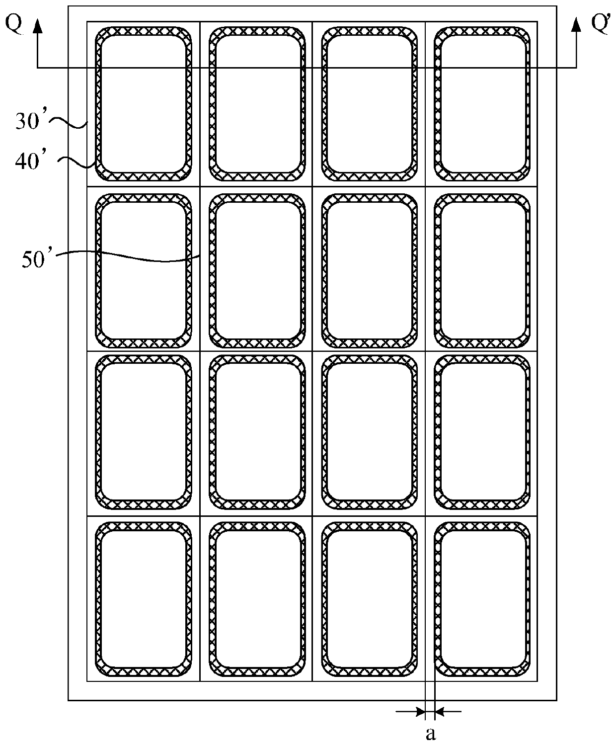
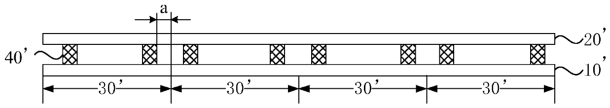
[0031] figure 1 It is a structural schematic diagram of a display motherboard in the prior art, figure 2 yes figure 1 The cross-sectional view along the QQ’ direction, such as figure 1 and figure 2 As shown, the existing display motherboard includes an organic light emitting display array motherboard 10' and a cover motherboard 20', and also includes a plurality of organic light emitting display panel regions 30'. Apply glass glue 40' on the cover motherboard 20' corresponding to the peripheral area of ​​eac...


PUM

PropertyMeasurementUnit
widthaaaaaaaaaa

Abstract

The embodiment of the invention discloses a display mother board and a preparation method of a display panel. The display mother board comprises an organic light-emitting display array mother board and a cover plate mother board, the organic light-emitting display array mother board comprises a plurality of organic light-emitting display panel areas, and each organic light-emitting display panel area comprises a display area and a peripheral area. A plurality of glass cement packaging structures are arranged between the organic light-emitting display array mother board and the cover plate mother board, a glass cement connecting part is arranged between the glass cement packaging structures corresponding to every two adjacent organic light-emitting display panel areas, and the adjacent glass cement packaging structures and the glass cement connecting parts between the adjacent glass cement packaging structures are connected into an integrated structure. The cover plate mother board is provided with a plurality of shading strips, the vertical projections of the shading strips on the cover plate mother board are located in the vertical projections of the glass cement connecting partson the cover plate mother board, and the vertical projections of cutting lines on the cover plate mother board are located in the vertical projections of the shading strips on the cover plate mother board. By adopting the technical scheme, the frame of the display panel can be reduced.

Description

technical field [0001] Embodiments of the present invention relate to the field of display technology, and in particular to a display motherboard and a method for preparing a display panel. Background technique [0002] Organic light-emitting display panels are widely used in various high-performance display fields due to their advantages of high brightness, low power consumption, wide viewing angle, high response speed, and wide operating temperature range. [0003] However, water vapor and oxygen in the surrounding environment seriously affect the lifetime of the OLED panel. Therefore, it is necessary to package the organic light emitting display panel. In the prior art, due to the existence of the packaging structure, it is not conducive to the narrow frame design of the organic light emitting display panel, and at the same time, it will cause a low utilization rate of the substrate of the display motherboard. Contents of the invention [0004] In view of this, an emb...

Claims


Application Information

Patent Timeline
Patent Type & Authority Applications(China)
IPC IPC(8): H01L51/52H01L51/56H01L27/32
CPCH10K59/10H10K50/8426H10K71/00
Inventor 陈敏刘昕昭
Owner WUHAN TIANMA MICRO ELECTRONICS CO LTD
Why Eureka
Try Eureka