
NAND memory and manufacturing method thereof

A manufacturing method and memory technology, applied in the field of memory, can solve problems such as film layer collapse, unstable channel structure, and affecting the support effect of the stack structure, and achieve the effect of ensuring stability and avoiding partial collapse of the film layer or the entire peeling off

Inactive Publication Date: 2020-04-21
YANGTZE MEMORY TECH CO LTD
View PDF3 Cites 1 Cited by
  • Summary
  • Abstract
  • Description
  • Claims
  • Application Information

AI Technical Summary

Problems solved by technology

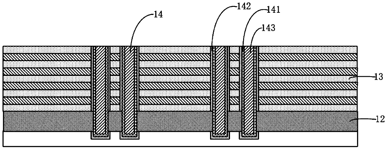
[0004] However, in order to realize the electrical connection between the channel and the common source channel, before the epitaxial layer is grown laterally on the side of the channel structure, the storage function layer on the outer side of the channel structure is wet-etched to expose the inner layer channel, and in the process of wet etching the outer surface of the channel structure, the semiconductor layer at the bottom of the channel structure will inevitably be corroded, and excessive erosion will lead to instability of the channel structure, In turn, it affects the support effect of the channel structure on the stack structure on the void area, so that the film layer in the stack structure is prone to local collapse or the entire peeling off problem

Method used


Image

  • NAND memory and manufacturing method thereof
  • NAND memory and manufacturing method thereof
  • NAND memory and manufacturing method thereof

Examples


Embodiment Construction

[0025] The present invention will be described in further detail below in conjunction with the accompanying drawings and embodiments. In particular, the following examples are only used to illustrate the present invention, but not to limit the scope of the present invention. Likewise, the following embodiments are only some of the embodiments of the present invention but not all of them. All other embodiments obtained by those skilled in the art without creative efforts all fall within the protection scope of the present invention.

[0026] In addition, the directional terms mentioned in the present invention, such as [top], [bottom], [front], [back], [left], [right], [inside], [outside], [side], etc., only is the direction with reference to the attached drawings. Therefore, the directional terms used are used to illustrate and understand the present invention, but not to limit the present invention. In the figures, structurally similar elements are denoted by the same refer...


PUM


Abstract

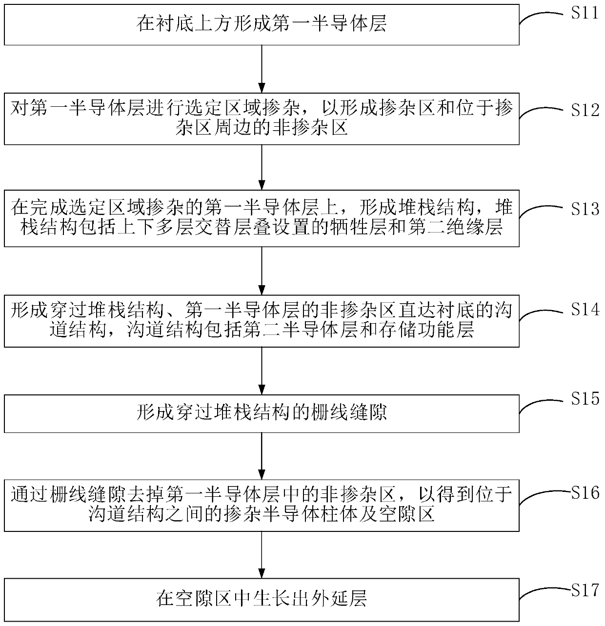
The invention relates to an NAND memory and a manufacturing method thereof. The manufacturing method comprises the following steps that: a first semiconductor layer is formed on a substrate; selectiveregion doping is performed on the first semiconductor layer, so that a doped region and a non-doped region located at the periphery of the doped region can be formed; a stack structure is formed on the first semiconductor layer which has been subjected to the selective region doping, wherein the stack structure comprises a plurality of sacrificial layers and a plurality of second insulating layers which are alternately stacked along a vertical direction; channel structures which penetrate through the stack structure and the non-doped region of the first semiconductor layer to directly reach the substrate are formed, wherein each channel structure comprises a second semiconductor layer and a storage function layer; grid line gaps passing through the stack structure are formed; the non-doped region in the first semiconductor layer are removed through the grid line gaps, so that a doped semiconductor column body and a gap region between the channel structures can be formed; and an epitaxial layer is grown in the gap region. Therefore, when the channel structures are eroded, the doped semiconductor column body positioned below the stack structure can provide auxiliary support, and therefore, the stability of the stack structure is ensured.

Description

【Technical field】 [0001] The invention relates to the technical field of memory, in particular to a NAND memory and a manufacturing method thereof. 【Background technique】 [0002] As technology develops, the semiconductor industry is constantly looking for new production methods to allow each memory die in a memory device to have a greater number of memory cells. Among them, 3D NAND (three-dimensional NAND) memory has become a cutting-edge three-dimensional memory technology with great development potential due to its advantages of high storage density and low cost. [0003] There is a 3D NAND memory including a substrate, an epitaxial layer and a stack structure disposed on the substrate in sequence, and a channel structure disposed in the stack structure and passing through the epitaxial layer to the substrate. The channel structure is included on the inner wall of the channel hole The storage function layer and the channel formed by the semiconductor film layer are arran...

Claims


Application Information

Patent Timeline
Patent Type & Authority Applications(China)
IPC IPC(8): H01L27/11524H01L27/11556H01L27/1157H01L27/11582H10B41/35H10B41/27H10B43/27H10B43/35
CPCH10B41/35H10B41/27H10B43/35H10B43/27
Inventor 刘小欣薛磊薛家倩耿万波黄波
Owner YANGTZE MEMORY TECH CO LTD
Learn More