
LCD touch display panel

A touch display panel, liquid crystal technology, applied in the directions of instruments, semiconductor devices, optics, etc., can solve problems such as affecting the performance of the touch display panel, prone to breakage, reducing the yield of the touch display panel, etc. The effect of breaking and eliminating cuts

Active Publication Date: 2022-07-29
WUHAN CHINA STAR OPTOELECTRONICS TECH CO LTD
View PDF8 Cites 0 Cited by
  • Summary
  • Abstract
  • Description
  • Claims
  • Application Information

AI Technical Summary

Problems solved by technology

[0005] The present invention provides a liquid crystal touch display panel, which can solve the problem that in the prior art, the common electrodes in the liquid crystal touch display panel form sharp corners on both sides of the metal wiring layer, the film layer is thin, and it is easy to break, thereby affecting the touch display. Panel performance, technical issues that reduce the yield of touch display panels

Method used


Image

  • LCD touch display panel
  • LCD touch display panel
  • LCD touch display panel

Examples


Embodiment Construction

[0022] The following descriptions of the various embodiments refer to the accompanying drawings to illustrate specific embodiments in which the invention may be practiced. The directional terms mentioned in the present invention, such as [up], [down], [front], [rear], [left], [right], [inner], [outer], [side], etc., are only for reference Additional schema orientation. Therefore, the directional terms used are for describing and understanding the present invention, not for limiting the present invention. In the figures, units with similar structures are denoted by the same reference numerals, and the dotted lines in the figures indicate that they do not exist in the structures, and only illustrate the shapes and positions of the structures.

[0023] The present invention aims at the formation of sharp corners on both sides of the metal wiring layer in the common electrode of the liquid crystal touch display panel in the prior art, the film layer is thin and prone to breakage,...


PUM


Abstract

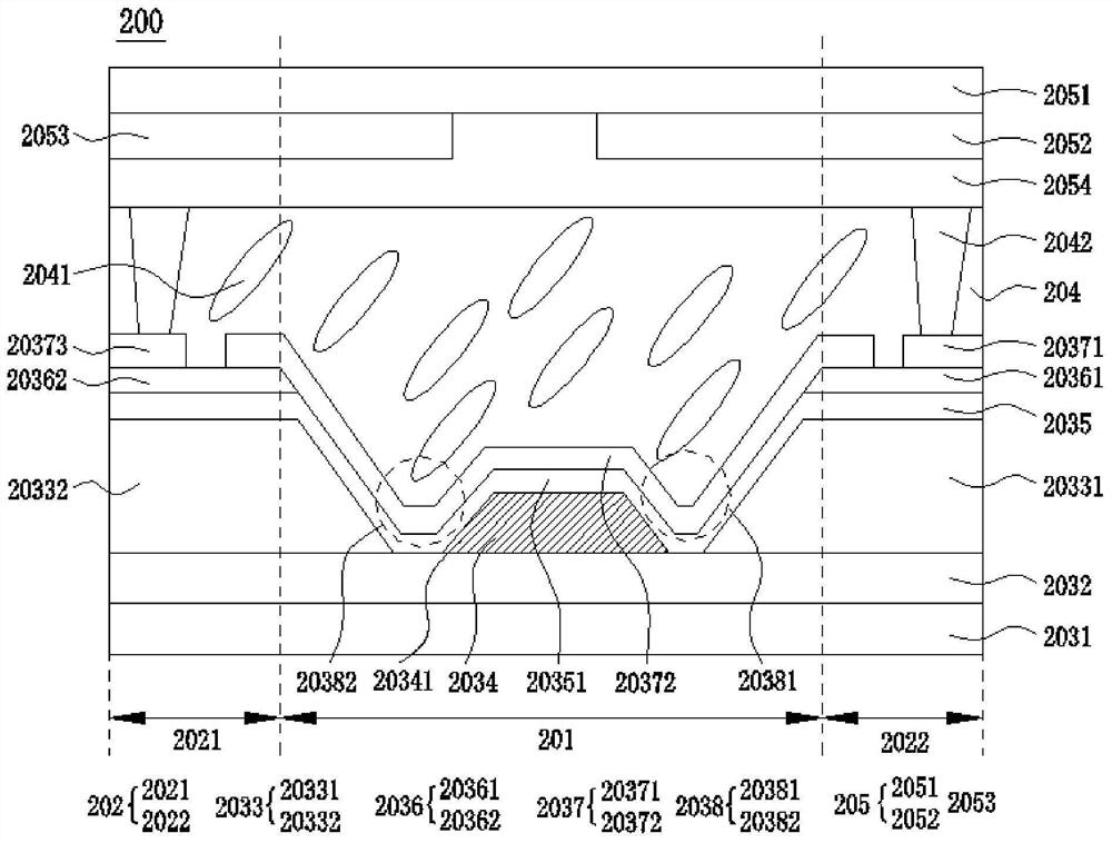
The present invention provides a liquid crystal touch display panel, which is provided with via holes on both sides of the opening area of ​​the planarization layer and the metal layer, and a reinforcing layer on the surface of the common electrode; the beneficial effects: compared with the existing liquid crystal touch display Panel, the present invention is provided with via holes on both sides of the opening area, and the wire exchange layer of the common electrode in the opening area is relatively gently bent and has less stress, which can effectively avoid fluctuations in the manufacturing process, eliminate the incision, and solve the problem that the common electrode is thin and easy to use. At the same time, a reinforcing layer is added on the surface of the wire exchange layer to increase the film thickness of the common electrode layer in the opening area, so as to further avoid the common electrode breakage and effectively improve the yield of the product.

Description

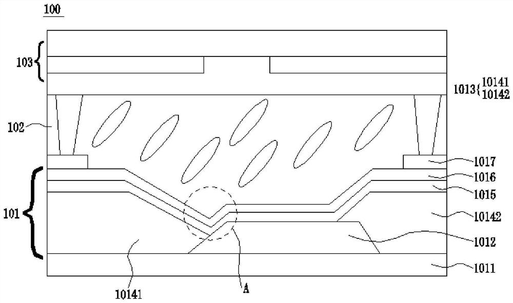
technical field [0001] The present invention relates to the field of display technology, and in particular, to a liquid crystal touch display panel. Background technique [0002] At present, the integrated touch display panel mainly includes two types: the on-cell type in which the touch sensor is arranged between the polarizer of the display panel and the color filter substrate; and the touch sensor embedded in In-Cell in the pixel structure of the display panel. [0003] figure 1 For existing in-cell touch display panels, such as figure 1 As shown, the touch display panel 100 includes an array substrate 101 , a color filter substrate 103 , and a liquid crystal layer 102 located between the array substrate 101 and the color filter substrate 103 . The wiring layer 1012 and the flattening layer 1013 covering the metal wiring layer 1012. The flattening layer 1013 includes the flattening layer 10141 and the flattening layer 10142. Due to the fluctuation, the process of open...

Claims


Application Information

Patent Timeline
Patent Type & Authority Patents(China)
IPC IPC(8): G02F1/1333G02F1/1335G02F1/1362H01L27/12
CPCG02F1/13338G02F1/133512G02F1/133514G02F1/136227H01L27/1244
Inventor 曹志浩
Owner WUHAN CHINA STAR OPTOELECTRONICS TECH CO LTD
Learn More