A kind of light oxidation method of algaas epitaxial layer
A technology of epitaxial layer and ultraviolet light, which is applied in the direction of lasers, laser components, semiconductor lasers, etc., can solve the problems of complex process, long time consumption, fluctuation of oxidation rate, etc., and achieve the effect of reducing complexity and cost
- Summary
- Abstract
- Description
- Claims
- Application Information
AI Technical Summary
Problems solved by technology
Method used
Image
Examples
Embodiment 1
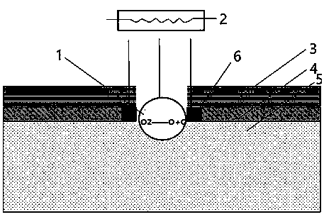
[0018] According to an embodiment of the present invention, as figure 1 As shown, a photo-oxidation method for an AlGaAs epitaxial layer mainly includes: an ultraviolet photocatalytic zone 1, an illumination device 2, a transmission epitaxial layer 3, an AlGaAs epitaxial layer 4, namely a target oxide layer, a GaAs substrate 5, and an infrared photocatalytic zone 6. Its steps include:
[0019] Step 1: On the GaAs substrate 5, grow an AlGaAs epitaxial layer 4 with a certain thickness, wherein the AlGaAs epitaxial layer 4 is an AlGaAs epitaxial layer containing a high Al composition, and the AlGaAs epitaxial layer 4 has a different oxidation levels. The AlGaAs epitaxial layer 4 is used as a target oxide layer, and a transmissive epitaxial layer 3 with a transmission wavelength less than 800 nm is grown on the AlGaAs epitaxial layer 4. The transmissive epitaxial layer 3 can protect the target oxide layer from natural oxidation. At the same time, in the photocatalytic reaction o...
Embodiment 2
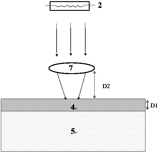
[0027] According to another embodiment proposed by the present invention, such as figure 2 As shown, a method for photo-oxidizing an AlGaAs epitaxial layer mainly includes: a microscope objective lens 7, an illumination device 2, an AlGaAs epitaxial layer 4, that is, a target oxide layer, and a GaAs substrate 5. Wherein, D2 is the distance between the microscope objective lens 7 and the AlGaAs epitaxial layer 4 , and D1 is the thickness of the AlGaAs epitaxial layer 4 . Include the following steps:
[0028] Step 1: On the GaAs substrate 5, grow an AlGaAs epitaxial layer 4 with a thickness of D2.
[0029] Step 2: The light beam emitted by the illumination device 2 passes through the microscope objective lens 7 to irradiate the AlGaAs epitaxial layer 4, that is, the high-energy ultraviolet light and infrared light emitted by the illumination device 2 are focused on the AlGaAs epitaxial layer 4 through the microscope objective lens 7, thereby accelerating the AlGaAs epitaxial l...
PUM
| Property | Measurement | Unit |
|---|---|---|
| wavelength | aaaaa | aaaaa |
| thickness | aaaaa | aaaaa |
Abstract
Description
Claims
Application Information
 - R&D Engineer
- R&D Manager
- IP Professional
- Industry Leading Data Capabilities
- Powerful AI technology
- Patent DNA Extraction
Browse by: Latest US Patents, China's latest patents, Technical Efficacy Thesaurus, Application Domain, Technology Topic, Popular Technical Reports.
© 2024 PatSnap. All rights reserved.Legal|Privacy policy|Modern Slavery Act Transparency Statement|Sitemap|About US| Contact US: help@patsnap.com


