Display panel and mask plate
A technology for display panels and masks, applied in ion implantation plating, coatings, electrical components, etc., can solve the problems of poor camera imaging quality and low pixel light transmittance, and achieve enhanced light transmittance and increased transmittance. Light area, the effect of improving image quality
- Summary
- Abstract
- Description
- Claims
- Application Information
AI Technical Summary
Problems solved by technology
Method used
Image
Examples
Embodiment Construction
[0028] The following descriptions of the various embodiments refer to the accompanying drawings to illustrate specific embodiments in which the invention may be practiced. The directional terms mentioned in the present invention, such as [top], [bottom], [front], [back], [left], [right], [inside], [outside], [side], etc., are only for reference The orientation of the attached schema. Therefore, the directional terms used are used to illustrate and understand the present invention, but not to limit the present invention. In the figures, structurally similar elements are denoted by the same reference numerals.
[0029] The present invention aims at that in the existing full-screen display panel, the light transmittance of pixels in the area corresponding to the camera on the display screen is low, which leads to poor imaging quality of the camera. The present invention can solve the above-mentioned problems.
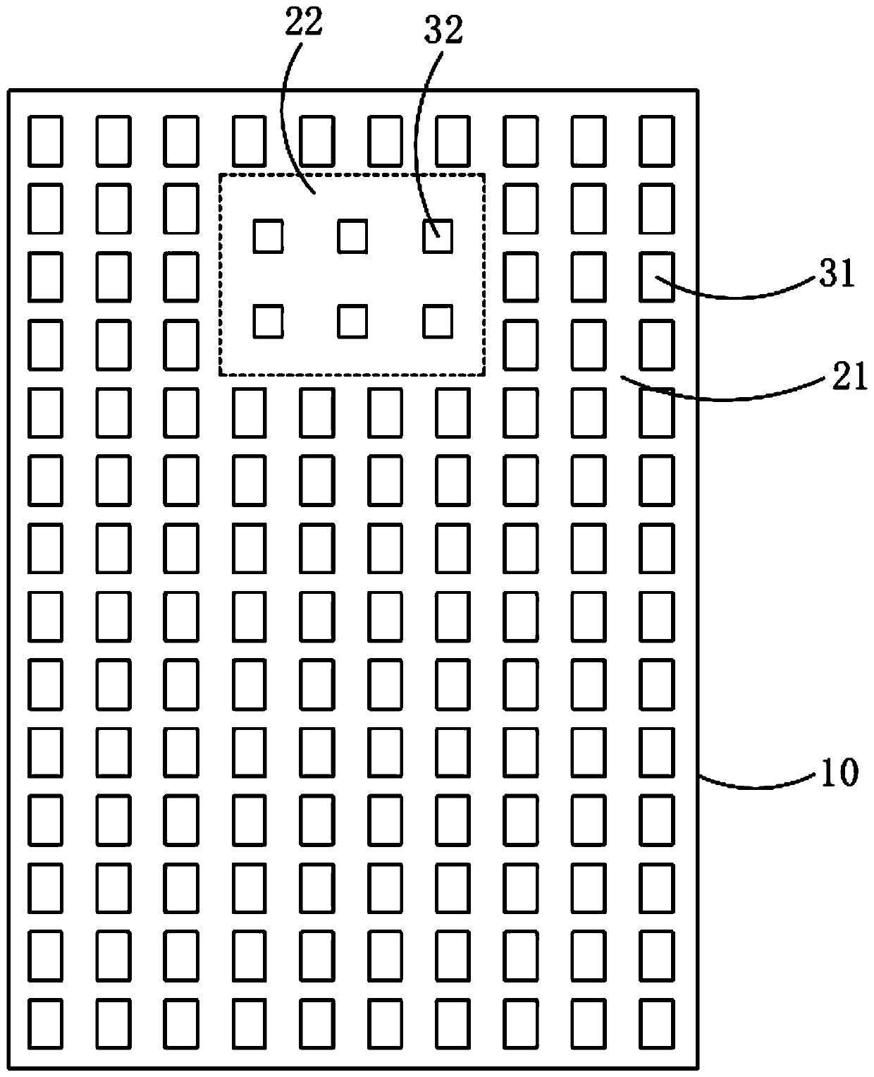
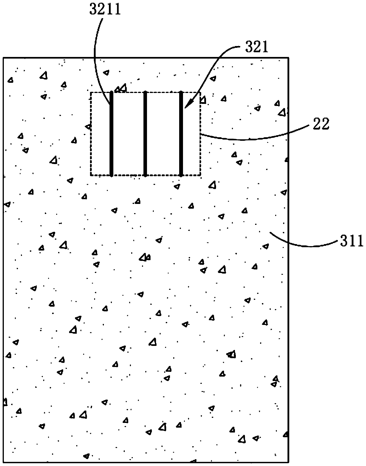
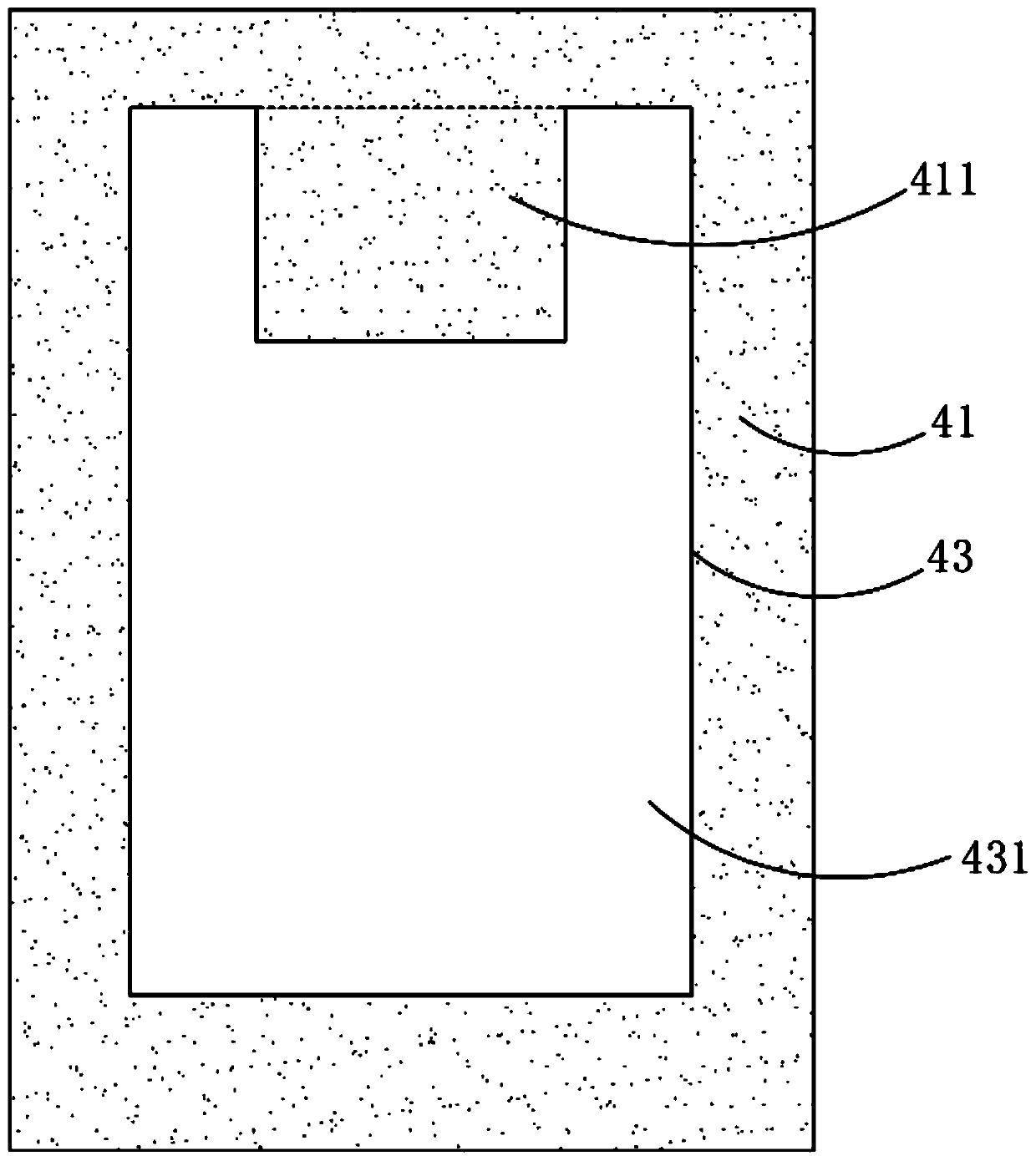
[0030] A display panel such as figure 1 As shown, the display pan...
PUM
 Abstract
Description
Claims
Application Information
 - R&D
- Intellectual Property
- Life Sciences
- Materials
- Tech Scout
- Unparalleled Data Quality
- Higher Quality Content
- 60% Fewer Hallucinations
Browse by: Latest US Patents, China's latest patents, Technical Efficacy Thesaurus, Application Domain, Technology Topic, Popular Technical Reports.
© 2025 PatSnap. All rights reserved.Legal|Privacy policy|Modern Slavery Act Transparency Statement|Sitemap|About US| Contact US: help@patsnap.com


