
Patsnap Eureka
For R&D, Patsnap Eureka makes reading and utilizing patents & technical documents easy.
Patsnap Eureka AIR
Designed for self-driven R&D workflows. Generate viable solutions, solve complex R&D challenges, empower your innovation with AI.

Patsnap Eureka Materials
Designed for material experts only. Revolutionize your material R&D, from search, analyze, to developing new materials.

TechResearch
Generate reliable direction feasibility study reports for your R&D in just a few steps.

TechSeek
Discover and master advanced knowledge NOW. Basics, ideas, possibilities, all at once.

TechMind
As an expert in R&D Theories, TechMind can generates customized viable solutions instantly.

TechRisk
Analyze your overall solution with one click, know your potential R&D risks in advance.

TechMonitor
Get weekly tech updates, stay abreast of the latest tech innovations and key insights.
Display panel and preparation method of the display panel
A display panel and bottom surface technology, which is applied in the direction of semiconductor devices, electrical components, circuits, etc., can solve the problems that the FMM opening area and the pixel cannot be completely aligned, the mask plate cannot be accurately positioned, and the display effect of the display panel is poor, so as to improve the display quality. effect, improve the aperture ratio and pixel resolution, and ensure the effect of accuracy
- Summary
- Abstract
- Description
- Claims
- Application Information
AI Technical Summary
Problems solved by technology
Method used
Image

Examples
Embodiment Construction
[0033] The technical solutions in the embodiments of the disclosure will be clearly and completely described below in conjunction with the drawings in the embodiments of the disclosure. Apparently, the described embodiments are only some of the embodiments of the present disclosure, not all of them. Based on the embodiments in the present disclosure, all other embodiments obtained by those skilled in the art without creative efforts fall within the protection scope of the present disclosure.
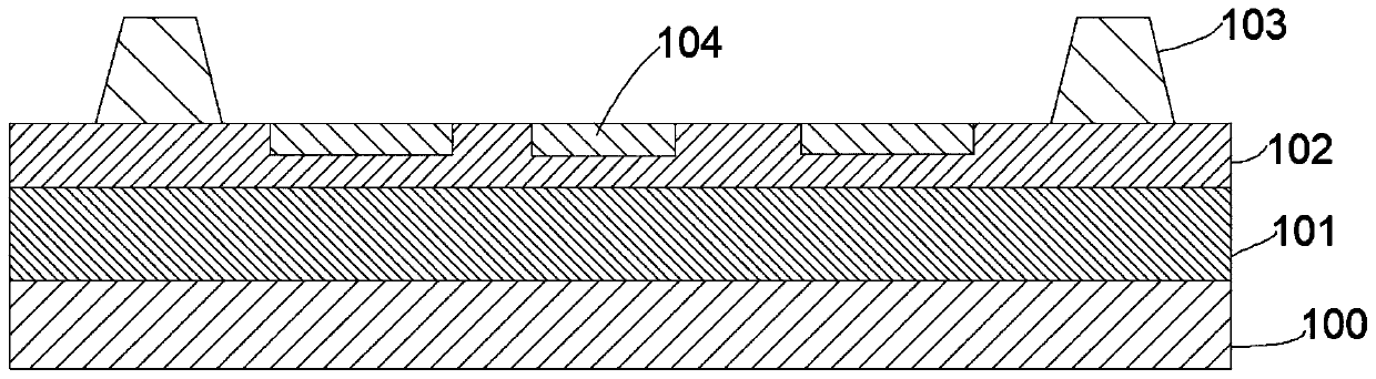
[0034] In the embodiment of the present disclosure, as figure 1 as shown, figure 1 It is a schematic diagram of the structure of each layer of the display panel of the disclosed embodiment. The display panel includes a base substrate 100 , an array substrate layer 101 , a pixel definition layer 102 and spacer columns 103 . The array substrate layer 101 is disposed on the base substrate 100 , the pixel definition layer 102 is disposed on the array substrate layer 101 , and the spacer c...
PUM
 Abstract
Description
Claims
Application Information
 - R&D Engineer
- R&D Manager
- IP Professional
- Industry Leading Data Capabilities
- Powerful AI technology
- Patent DNA Extraction
Browse by: Latest US Patents, China's latest patents, Technical Efficacy Thesaurus, Application Domain, Technology Topic, Popular Technical Reports.
© 2024 PatSnap. All rights reserved.Legal|Privacy policy|Modern Slavery Act Transparency Statement|Sitemap|About US| Contact US: help@patsnap.com