
Light-transmitting display panel, manufacturing method thereof, and display panel

A technology for display panels and manufacturing methods, applied in semiconductor/solid-state device manufacturing, diodes, organic semiconductor devices, etc., can solve the problems of not being full-screen, not being able to display on the screen, and not being able to display pictures by the front camera, to achieve high color accuracy, The effect of improving light transmission performance

Active Publication Date: 2022-04-19
KUNSHAN GO VISIONOX OPTO ELECTRONICS CO LTD
View PDF11 Cites 0 Cited by
  • Summary
  • Abstract
  • Description
  • Claims
  • Application Information

AI Technical Summary

Problems solved by technology

However, these electronic devices are not truly full-screen, and cannot be displayed in all areas of the entire screen. For example, the corresponding area of ​​​​the front camera cannot display images.

Method used


Image

  • Light-transmitting display panel, manufacturing method thereof, and display panel
  • Light-transmitting display panel, manufacturing method thereof, and display panel
  • Light-transmitting display panel, manufacturing method thereof, and display panel

Examples


Embodiment Construction

[0044]The characteristics and exemplary embodiments of various aspects of the present invention will be described in detail below. In order to make the purpose, technical solutions and advantages of the present invention clearer, the present invention will be further described in detail below in conjunction with the accompanying drawings and specific embodiments. It should be understood that the specific embodiments described here are only configured to explain the present invention, not to limit the present invention. It will be apparent to one skilled in the art that the present invention may be practiced without some of these specific details. The following description of the embodiments is only to provide a better understanding of the present invention by showing examples of the present invention.

[0045] It should be noted that in this article, relational terms such as first and second are only used to distinguish one entity or operation from another entity or operation,...


PUM

PropertyMeasurementUnit
transmittivityaaaaaaaaaa

Abstract

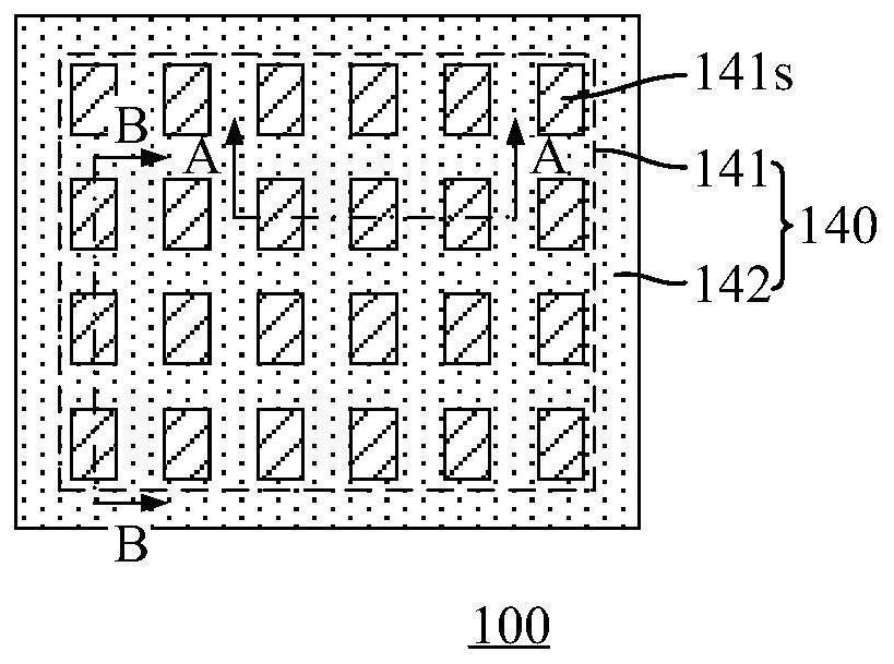
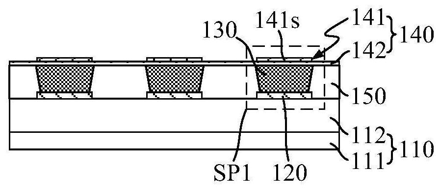
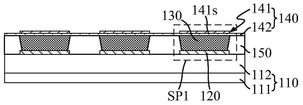
The invention discloses a light-transmitting display panel, a manufacturing method thereof, and a display panel. The light-transmitting display panel includes: an array substrate; a first electrode located on the array substrate; a first light-emitting structure located on the first electrode; and a second electrode layer group located on the first light-emitting structure, the second electrode layer group includes mutual The stacked first sub-electrode layer and the second sub-electrode layer, wherein the first sub-electrode layer includes electrode blocks spaced apart from each other, and the orthographic projection of each electrode block on the array substrate covers at least one first electrode on the array substrate The orthographic projection of the second sub-electrode layer is connected to at least part of the adjacent electrode blocks, and the light transmission capacity of the second sub-electrode layer is greater than that of the electrode blocks. According to the light-transmitting display panel of the embodiments of the present invention, while ensuring the normal display of the sub-pixels, the light-transmitting performance of the non-light-emitting areas around the sub-pixels is improved.

Description

technical field [0001] The invention relates to the display field, in particular to a light-transmitting display panel, a manufacturing method thereof, and a display panel. Background technique [0002] With the rapid development of electronic devices, users have higher and higher requirements for screen-to-body ratio, so that the full-screen display of electronic devices has attracted more and more attention from the industry. [0003] Traditional electronic devices, such as mobile phones and tablet computers, need to integrate front-facing cameras, earpieces, and infrared sensing elements. In the prior art, a notch or hole can be made on the display screen, and external light can enter the photosensitive element located below the screen through the notch or hole on the screen. However, none of these electronic devices is a full screen in the true sense, and cannot be displayed in all areas of the entire screen, for example, the area corresponding to the front camera canno...

Claims


Application Information

Patent Timeline
Patent Type & Authority Patents(China)
IPC IPC(8): H01L51/52H01L27/32H01L51/56
CPCH10K59/12H10K50/82H10K71/00H10K59/65H10K59/121H10K50/822H10K50/828H10K50/813H10K2102/103
Inventor 彭兆基刘明星王盼盼李伟丽甘帅燕
Owner KUNSHAN GO VISIONOX OPTO ELECTRONICS CO LTD
Learn More