OLED display panel and display device

A technology for display panels and display areas, which is applied in the manufacturing of electrical components, electrical solid-state devices, and semiconductor/solid-state devices, etc., can solve the problems of poor encapsulation effect of the encapsulation layer in the test area, and achieve the effect of enhancing the encapsulation effect

Active Publication Date: 2020-02-28
SHENZHEN CHINA STAR OPTOELECTRONICS SEMICON DISPLAY TECH CO LTD
View PDF8 Cites 4 Cited by
  • Summary
  • Abstract
  • Description
  • Claims
  • Application Information

AI Technical Summary

Problems solved by technology

[0005] This disclosure provides an OLED display panel and a display device to alleviate the technical problem of poor encapsulation effect of the encapsulation layer in the existing test area

Method used


Image

  • OLED display panel and display device
  • OLED display panel and display device
  • OLED display panel and display device

Examples


Embodiment Construction

[0023] The following descriptions of the various embodiments refer to the accompanying drawings to illustrate specific embodiments in which the present disclosure may be practiced. The directional terms mentioned in this disclosure, such as [top], [bottom], [front], [back], [left], [right], [inside], [outside], [side], etc., are for reference only The orientation of the attached schema. Therefore, the directional terms used are used to explain and understand the present disclosure, but not to limit the present disclosure. In the figures, structurally similar elements are denoted by the same reference numerals.

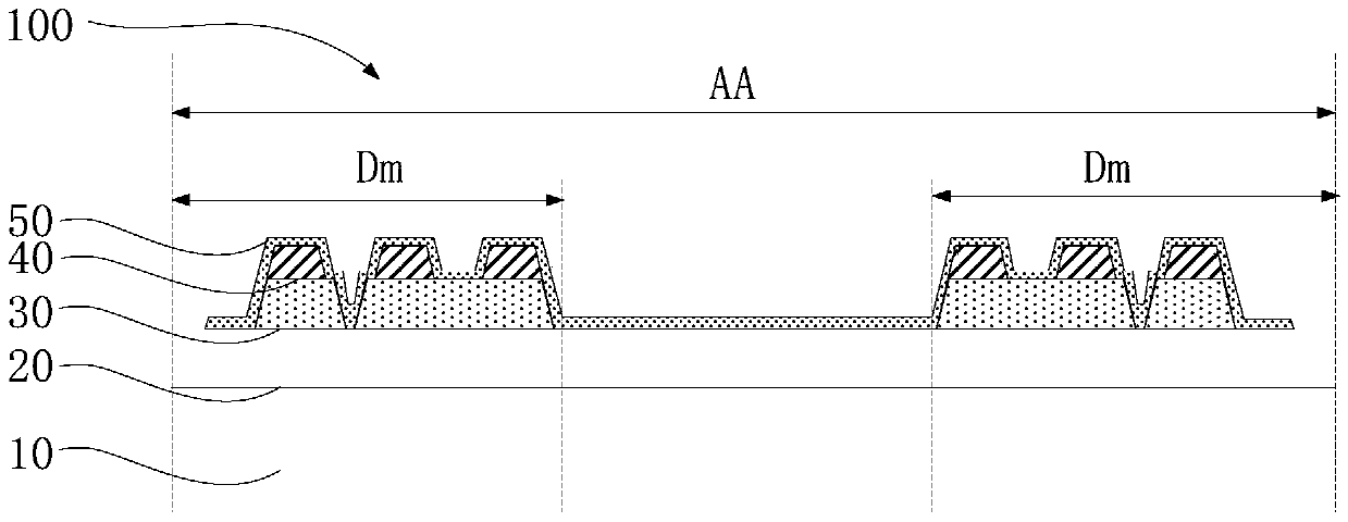
[0024] In one embodiment, as figure 1 As shown, an OLED display panel 100 is provided, a test area Dm is set in a display area AA of the OLED display panel, and the test area Dm is located at the edge of the display area AA. The test area Dm includes a substrate 10 , an inorganic film layer 20 , a planarization layer 30 , a pixel definition layer 40 , and an encapsu...


PUM


Abstract

The invention provides an OLED display panel and a display device. A test area of the OLED display panel comprises a substrate, an inorganic film layer, a planarization layer, a pixel definition layerand a packaging layer which are laminated, wherein the planarization layer is provided with a through hole at a pixel opening position corresponding to the pixel definition layer, and the packaging layer is deposited in the pixel opening and the through hole; and the planarization layer is separated from each other to form a new water blocking area and the packaging effect is enhanced.

Description

technical field [0001] The disclosure relates to the field of display technology, and in particular to an OLED display panel and a display device. Background technique [0002] For the technology of making OLED light-emitting devices by inkjet printing (Ink Jet Printing, IJP) process, since the film thickness at the edge of the light-emitting area is different from the film thickness at the center of the light-emitting area during printing, it is necessary to print an additional test area to ensure effective The uniformity of film thickness in the light-emitting area. However, the test area is composed of organic materials such as pixel definition layer and planarization layer, and the test area is inside the encapsulation area and close to the edge of the encapsulation area. Due to the poor water resistance of organic materials, water vapor is more likely to invade the OLED light-emitting device through the test area. [0003] The bottom of the existing test area is an ino...

Claims


Application Information

Patent Timeline
Patent Type & Authority Applications(China)
IPC IPC(8): H01L51/52
CPCH10K50/84
Inventor 杨中国李金川
Owner SHENZHEN CHINA STAR OPTOELECTRONICS SEMICON DISPLAY TECH CO LTD
Why Eureka
Try Eureka