Deep ultraviolet led structure and its manufacturing method
A technology of LED structure and manufacturing method, which is applied in the direction of semiconductor devices, electrical components, circuits, etc., can solve problems such as the reduction of external quantum efficiency of deep ultraviolet LEDs, and achieve the effect of improving external quantum efficiency
- Summary
- Abstract
- Description
- Claims
- Application Information
AI Technical Summary
Problems solved by technology
Method used
Image
Examples
no. 1 example
[0076] In a first exemplary embodiment of the present disclosure, a deep ultraviolet LED structure is provided.
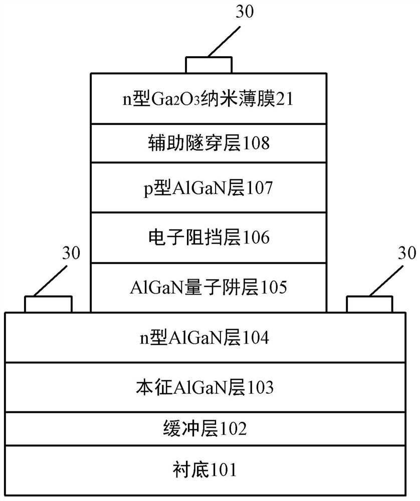
[0077] figure 1 It is a schematic diagram of a deep ultraviolet LED structure according to an embodiment of the present disclosure.
[0078] refer to figure 1 As shown, the deep ultraviolet LED structure of the present disclosure includes: a deep ultraviolet AlGaN epitaxial structure 10, including: a p-type AlGaN layer 107; an n-type Ga 2 o 3 Nano film 21, located on the upper surface of the deep ultraviolet AlGaN epitaxial structure 10; wherein, the n-type Ga 2 o 3 The nano film 21 forms a tunnel junction with the p-type AlGaN layer 107, serving as a surface electrode contact layer and a hole supply layer.
[0079] The n-type Ga 2 o 3 The nano film is on the order of hundreds of nanometers, such as in this embodiment, the n-type Ga 2 o 3 The thickness of the nano film 21 is 10 nanometers to 10 micrometers.
[0080] By using n-type Ga 2 o 3 The nano fil...
no. 2 example
[0107] In a second exemplary embodiment of the present disclosure, a method for fabricating a deep ultraviolet LED structure is provided.
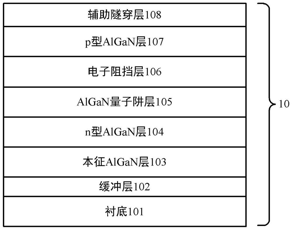
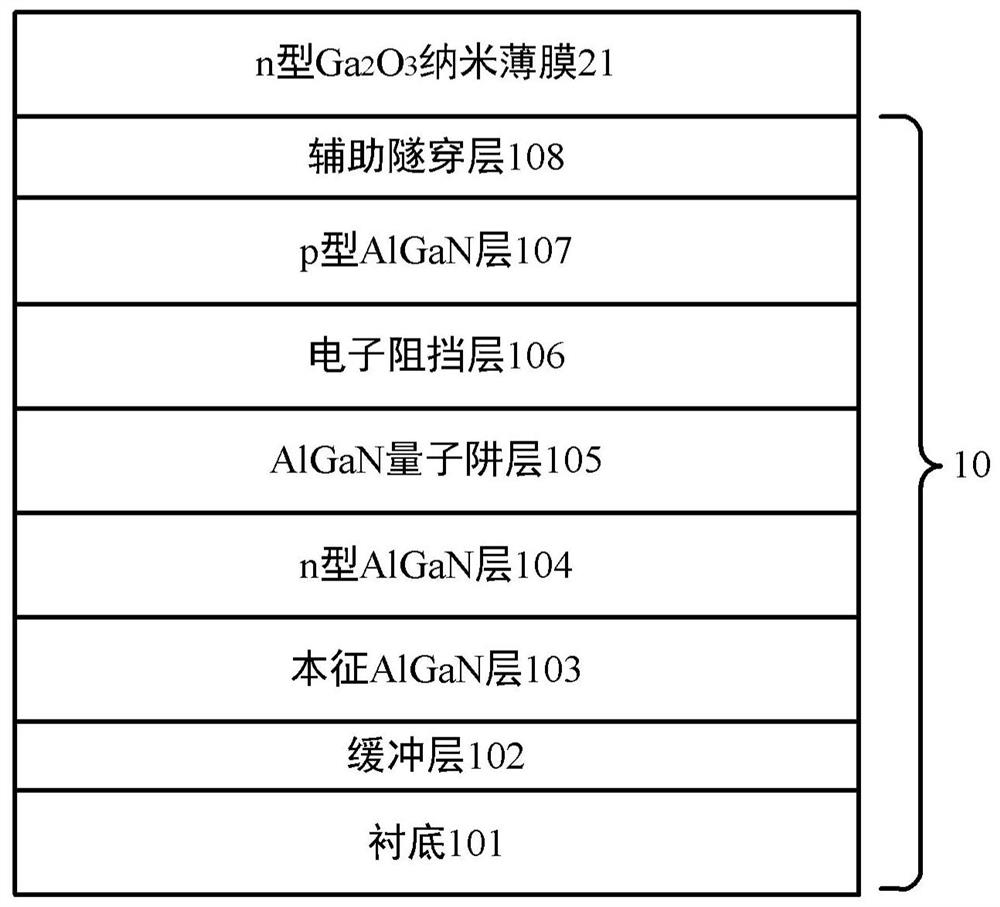
[0108] Figure 2-Figure 5 Each is a schematic diagram of the implementation process of each step corresponding to the manufacturing method of the deep ultraviolet LED structure shown in an embodiment of the present disclosure. in, figure 2 It is a schematic diagram of preparing a deep ultraviolet AlGaN epitaxial structure. image 3 n-type Ga 2 o 3 Schematic diagram of the transfer of nanofilms to the surface of deep-ultraviolet AlGaN epitaxial structures. Figure 4 for n-type Ga 2 o 3 Schematic illustration of the nanofilm etched down to the n-type AlGaN layer to make the mesa. Figure 5 Schematic diagram for forming electrodes on the mesas to form a deep-UV LED structure.
[0109] refer to Figure 2-Figure 5 As shown, the manufacturing method of the deep ultraviolet LED structure of the present disclosure includes:
[0110] Ste...
PUM
| Property | Measurement | Unit |
|---|---|---|
| thickness | aaaaa | aaaaa |
| thickness | aaaaa | aaaaa |
| thickness | aaaaa | aaaaa |
Abstract
Description
Claims
Application Information
 - R&D
- Intellectual Property
- Life Sciences
- Materials
- Tech Scout
- Unparalleled Data Quality
- Higher Quality Content
- 60% Fewer Hallucinations
Browse by: Latest US Patents, China's latest patents, Technical Efficacy Thesaurus, Application Domain, Technology Topic, Popular Technical Reports.
© 2025 PatSnap. All rights reserved.Legal|Privacy policy|Modern Slavery Act Transparency Statement|Sitemap|About US| Contact US: help@patsnap.com


