Lip seal with improved byproduct deposition problem and semiconductor processing device containing same

A technology for engineering devices and by-products, applied in the field of semiconductor engineering devices, can solve problems such as increased leakage, decreased substrate engineering uniformity, incomplete contact, etc., to prevent uniformity decrease, prevent incomplete contact, and reduce heat transfer gas leaked effect

Active Publication Date: 2020-01-07
GIGALANE CO LTD
View PDF10 Cites 0 Cited by
  • Summary
  • Abstract
  • Description
  • Claims
  • Application Information

AI Technical Summary

Problems solved by technology

[0009] Due to this by-product of vapor deposition on the lip seal, there is a problem of incomplete contact when the substrate is in contact with the lip seal
[0010] Furthermore, the amount of leakage of heat transfer gas to the parts where the substrate and the lip seal are not in complete contact increases
[0011] The increase in the leakage of the heat transfer gas will cause a temperature difference between the part where the leakage of the heat transfer gas increases and the part where the leakage of the heat transfer gas does not increase, and this temperature difference will eventually cause the uniformity of the substrate process to decrease. question

Method used


Image

  • Lip seal with improved byproduct deposition problem and semiconductor processing device containing same
  • Lip seal with improved byproduct deposition problem and semiconductor processing device containing same
  • Lip seal with improved byproduct deposition problem and semiconductor processing device containing same

Examples


Embodiment Construction

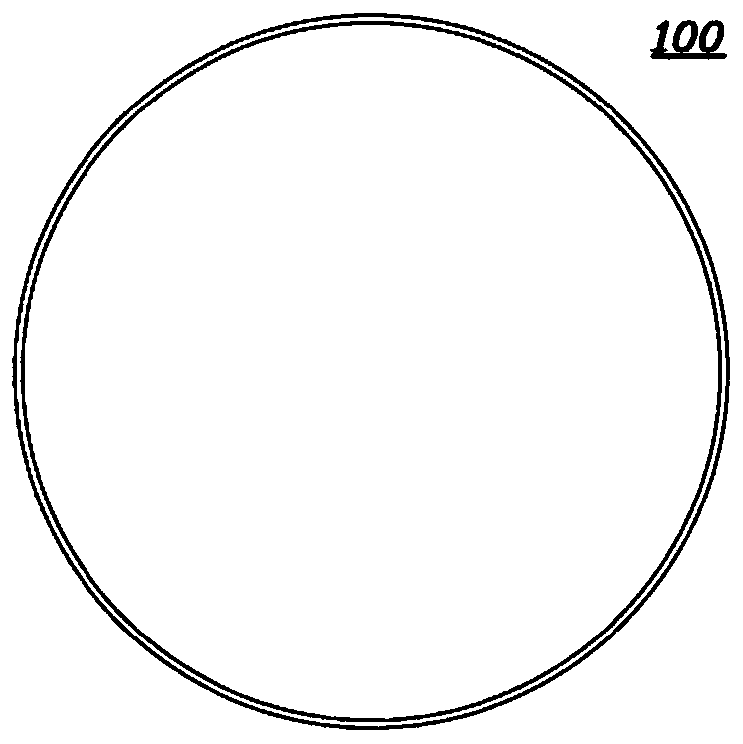
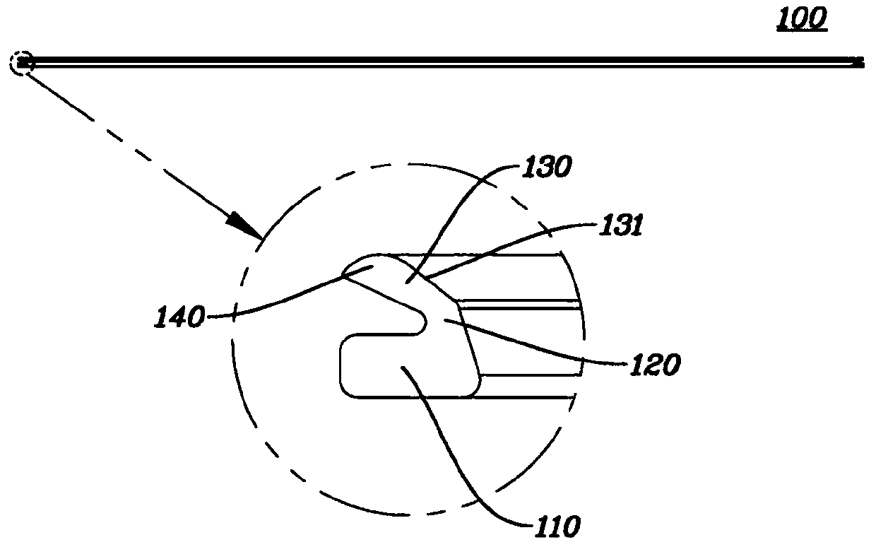
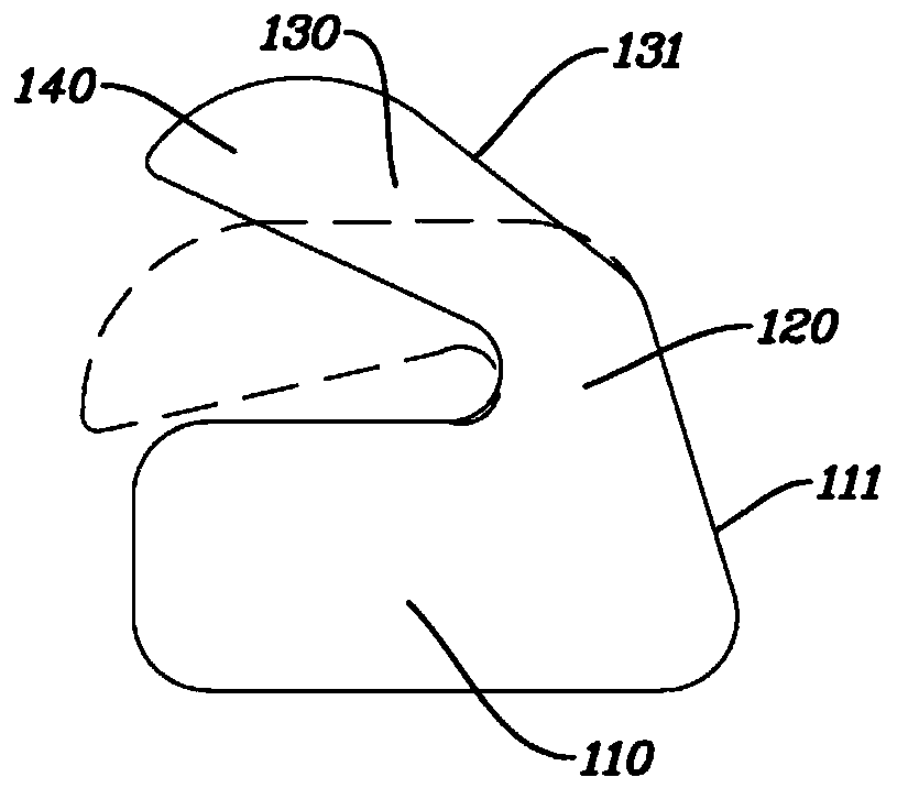
[0048] The lip seal which improves the problem of by-product vapor deposition and the semiconductor engineering device including the lip seal of the present invention will be described in detail below with reference to the accompanying drawings.

[0049] By-products generated during the semiconductor process of the substrate S are vapor-deposited on the lip seal 100 .

[0050] Due to this by-product evaporated on the lip seal 100, there is a problem of incomplete contact when the substrate S is in contact with the lip seal 100.

[0051] Furthermore, the leakage amount of the heat transfer gas to the portion where the substrate S and the lip seal 100 do not completely contact increases.

[0052] This increase in the leakage of heat transfer gas will cause a temperature difference between the portion of the substrate S where the leakage of heat transfer gas has increased and the portion where the leakage of heat transfer gas has not increased, and this temperature difference wil...


PUM


Abstract

The present invention relates to a semiconductor processing device having a lip seal with an improved byproduct deposition problem, which comprises: a support unit formed to be ring-shaped, and havinga hollow portion at an internal side thereof; an elastic unit extending from an upper surface of the support unit; a contact unit extending from one end of the elastic unit, and having a flat area onan upper surface thereof; and a sliding unit extending from one end of the contact unit. Moreover, an upper surface of the sliding unit is formed to be round-shaped.

Description

technical field [0001] The invention relates to a lip seal which improves the problem of vapor deposition of by-products and a semiconductor engineering device comprising the lip seal. Background technique [0002] Tong Semiconductor Processing Equipment is a device that places substrates on chucks and processes substrates through semiconductor processing. [0003] For example, an apparatus for processing a substrate by semiconductor processing may be an apparatus that performs one or more of etching, vapor deposition, and ashing with plasma, or a device that performs vapor deposition with a metal gas. [0004] The substrate may refer to a wafer or a tray on which a wafer is mounted. [0005] In such a semiconductor process apparatus, since a semiconductor process is performed in a chamber in a vacuum state, an inert gas as a heat transfer gas is supplied from a chuck to a substrate for heat regulation of the substrate. [0006] At this time, a lip seal is interposed betwe...

Claims


Application Information

Patent Timeline
IPC IPC(8): H01J37/32H01L21/687H01L21/67
CPCH01J37/32724H01L21/67248H01L21/68785H01L21/67017H01L21/67126H01L21/683
Inventor 金亨源郑明教郑熙锡
Owner GIGALANE CO LTD
Why Eureka
Try Eureka