Shell assembly and preparation method thereof and electronic equipment
A technology for shell components and electronic equipment, which is applied in the direction of electrical equipment shell/cabinet/drawer, branch equipment, electronic equipment, etc., can solve the problem of destroying the appearance consistency of the shell, and achieve good appearance consistency effect and appearance consistency effect. Good, the effect of eliminating appearance differences
- Summary
- Abstract
- Description
- Claims
- Application Information
AI Technical Summary
Problems solved by technology
Method used
Image
Examples
preparation example Construction
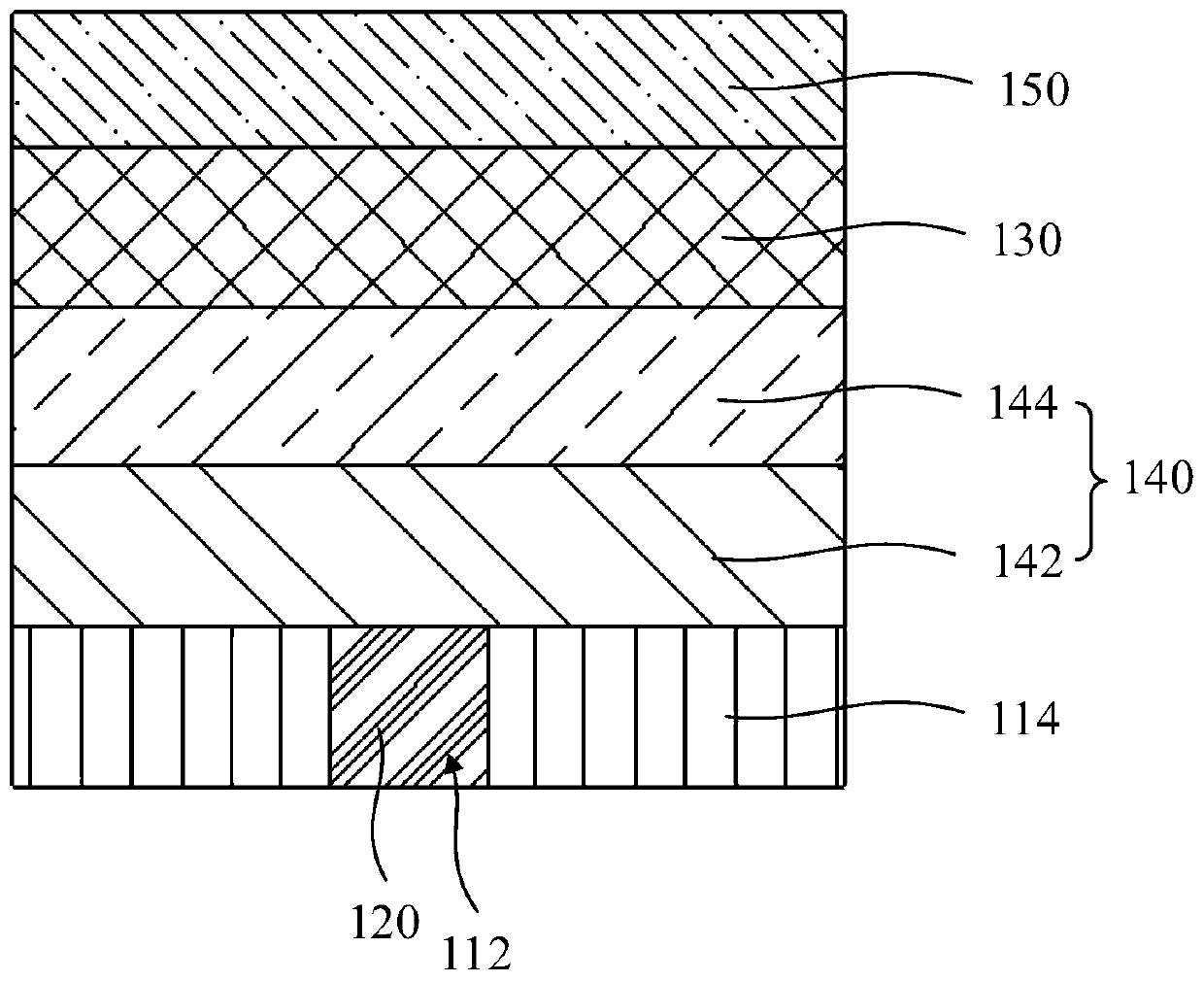
[0101] In the manufacturing method of the housing assembly 100 of the above-mentioned embodiment, by arranging the plastic part 120 in the accommodating hole 112, the plastic part 120 is fixed to the base 110, and the covering layer 130 is formed on the display surface, and the covering layer 130 covers the accommodating hole The opening of 112 on the display surface can eliminate the appearance difference between the plastic part 120 and the base 110, so that the shell assembly 100 has a better appearance consistency effect on the display surface. The above housing assembly 100 has better signal receiving performance and better appearance consistency.
[0102] Further, in the above-mentioned preparation method of the housing assembly 100, the ceramic material is sprayed on the display surface to form the covering layer 130, so that the housing assembly 100 has a ceramic texture and does not interfere with signals, and can be obtained by selecting different ceramic materials. ...
Embodiment 1
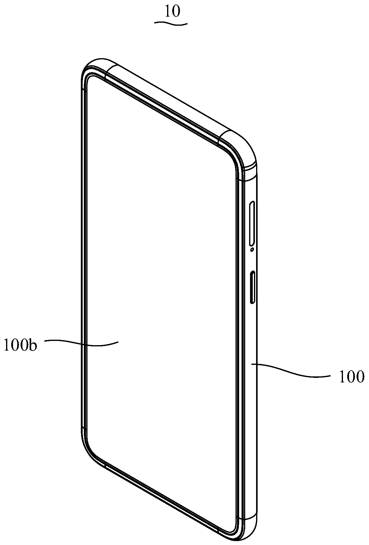
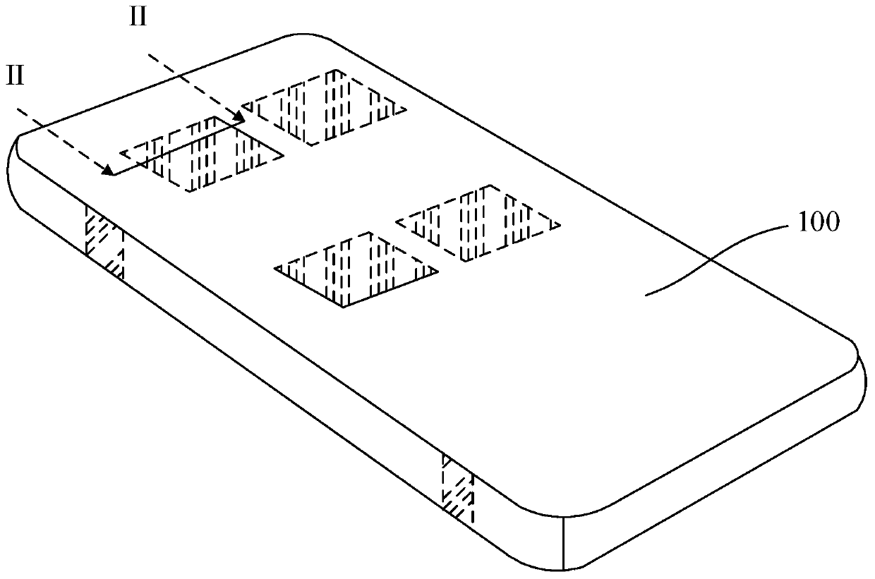
[0111] The structure of the shell assembly of the present embodiment is as Figure 1~5 shown. The preparation process of the shell assembly of the present embodiment is as follows:
[0112] (1) A base is provided, the base has a display surface, and a through accommodating hole is opened on the base, and an opening of the accommodating hole is located on the display surface.
[0113] (2) A nano-injection molding process is used to arrange plastic parts in the accommodating hole, and the plastic parts are fixedly connected to the base. The display surface of the substrate is roughened, and the surface roughness of the roughened display surface is 1 μm.
[0114] (3) An isolation layer is formed on the display surface by means of PVD, the isolation layer completely covers the display surface, and the shielding accommodating hole is located at the opening of the display surface. The material of the isolation layer is aluminum nitride, and the thickness of the isolation layer is...
Embodiment 2
[0119] The structure of the shell assembly of the present embodiment is as Figure 1~5 shown. The preparation process of the shell assembly of the present embodiment is as follows:
[0120] (1) A base is provided, the base has a display surface, and a through accommodating hole is opened on the base, and an opening of the accommodating hole is located on the display surface.
[0121] (2) A nano-injection molding process is used to arrange plastic parts in the accommodating hole, and the plastic parts are fixedly connected to the base. The display surface of the substrate is roughened, and the surface roughness of the roughened display surface is 1 μm.
[0122] (3) An isolation layer is formed on the display surface by means of PVD, the isolation layer completely covers the display surface, and the shielding accommodating hole is located at the opening of the display surface. The material of the isolation layer is aluminum oxide and silicon nitride. The thickness of the iso...
PUM
| Property | Measurement | Unit |
|---|---|---|
| thickness | aaaaa | aaaaa |
| thickness | aaaaa | aaaaa |
| thickness | aaaaa | aaaaa |
Abstract
Description
Claims
Application Information
 - Generate Ideas
- Intellectual Property
- Life Sciences
- Materials
- Tech Scout
- Unparalleled Data Quality
- Higher Quality Content
- 60% Fewer Hallucinations
Browse by: Latest US Patents, China's latest patents, Technical Efficacy Thesaurus, Application Domain, Technology Topic, Popular Technical Reports.
© 2025 PatSnap. All rights reserved.Legal|Privacy policy|Modern Slavery Act Transparency Statement|Sitemap|About US| Contact US: help@patsnap.com


